Laser planarization efficiency and roughness of CVD diamond film
-
摘要: 对化学气相沉积(CVD)多晶金刚石膜进行激光平整化的正交试验,使用场发射环境扫描电子显微镜(SEM)进行形貌分析,激光共聚焦扫描显微镜测量线粗糙度Ra、面粗糙度Sa和切缝锥度,分析激光参数对CVD膜平整化的影响。结果表明:影响切缝锥度的因素依次为脉冲宽度、脉冲频率、进给速度和激光电流,影响线粗糙度Ra的因素依次为进给速度、激光电流、脉冲频率、脉冲宽度。正交试验优化后,当激光电流为64 A、脉冲宽度为400 μs、脉冲频率为275 Hz、进给速度为100 mm/min时,可获得最佳的切槽表面形貌。采用该优化参数进行面扫描,测得面粗糙度Sa为11.7 μm;进一步增加入射角度至75°时,面粗糙度Sa降低至1.9 μm,实际去除效率达到1.1 mm3/min。Abstract: The orthogonal experiment of laser planarization of CVD polycrystalline diamond film was carried out, and the morphology was analyzed by using scanning electron microscope (SEM). The surface roughness Ra, the surface roughness Sa and the taper of kerf were measured by confocal laser scanning microscope. The influence of laser parameters on cutting quality was analyzed. The results show that the factors affecting kerf taper are pulse width, pulse frequency, feed speed and laser current in turn, and the factors affecting line roughness are feed speed, laser current, pulse frequency and pulse width in turn. After optimization by orthogonal test, the best groove surface morphology can be obtained with laser current of 64 A, pulse width of 400 μs, pulse frequency of 275 Hz and feed speed of 100 mm/min. Using the optimized parameters, the surface roughness Sa was measured to be 11.7 μm. When the incident angle increased to 75°, the surface roughness Sa decreased to 1.9 μm, and the actual removal efficiency reached 1.1 mm3/min.
-
Key words:
- CVD diamond film /
- laser planarization /
- surface roughness /
- mechanical grinding
-
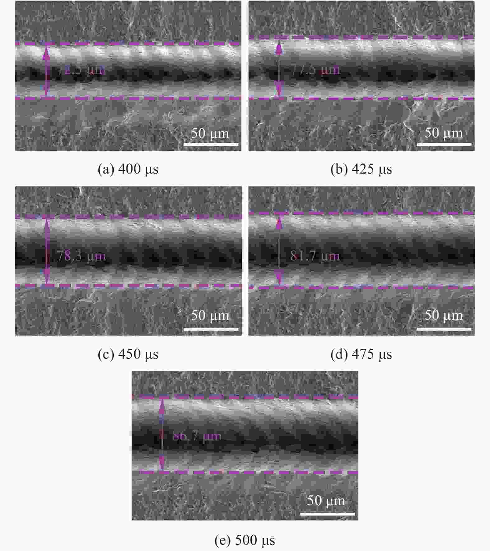
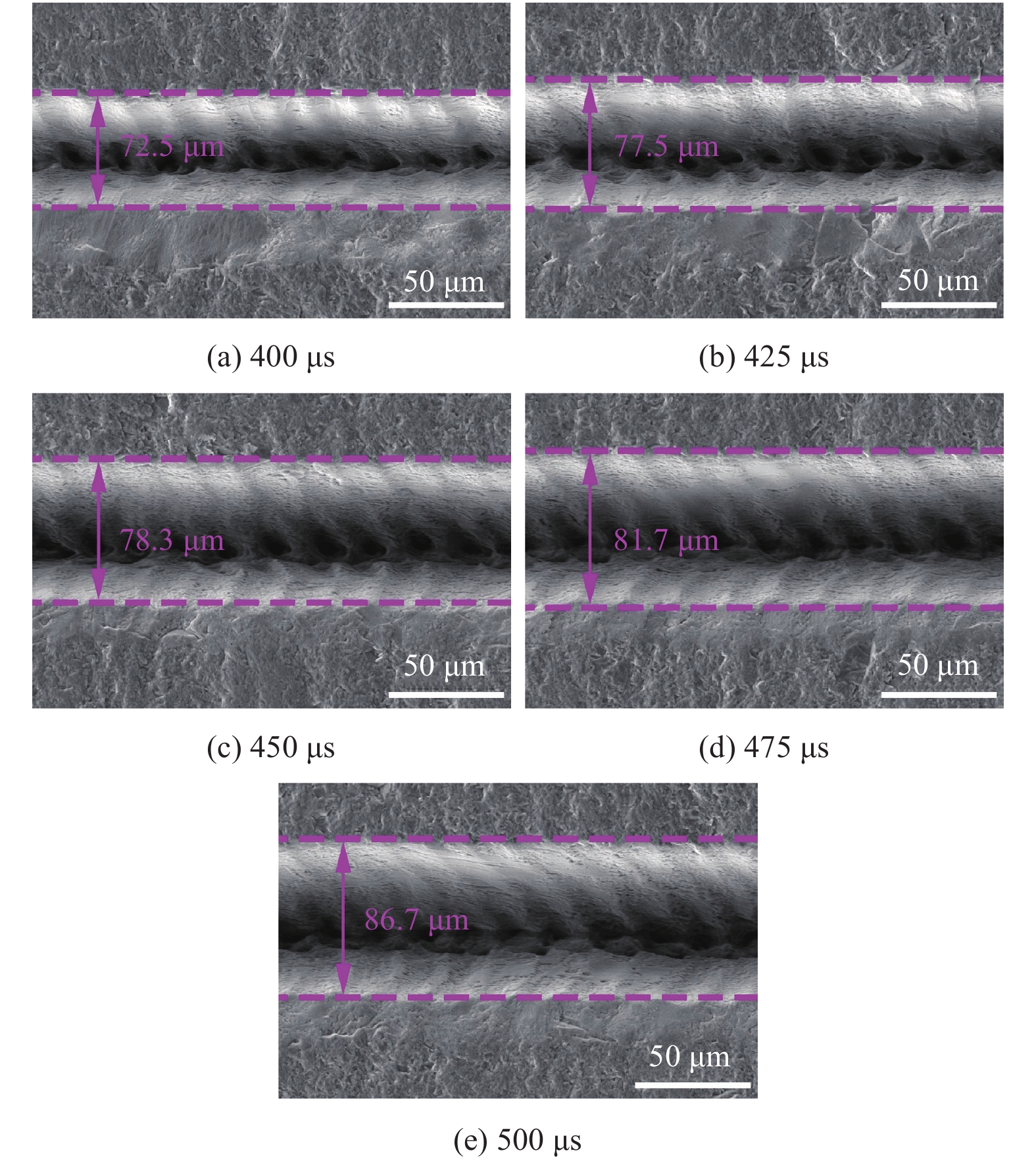
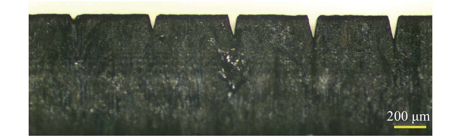
图 3 不同脉冲宽度对切缝的形貌影响
Figure 3. Influence of different laser pulse width on the morphology of the kerf
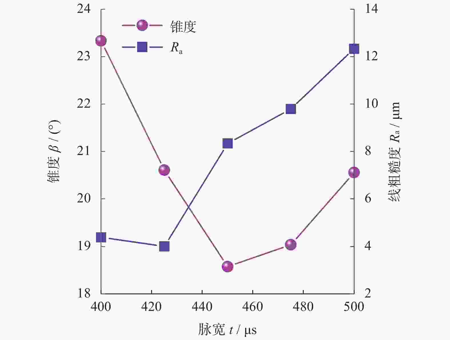
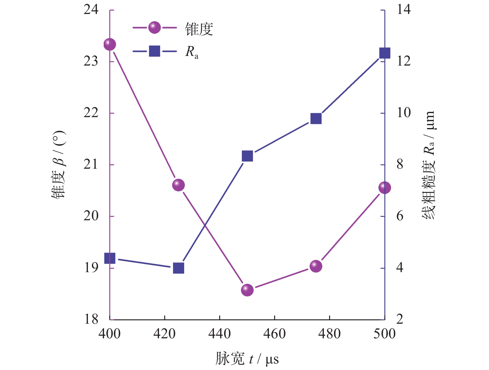
图 4 切缝锥度和线粗糙度Ra随脉冲宽度变化曲线
Figure 4. Curves of taper and roughness Ra changing with pulse width
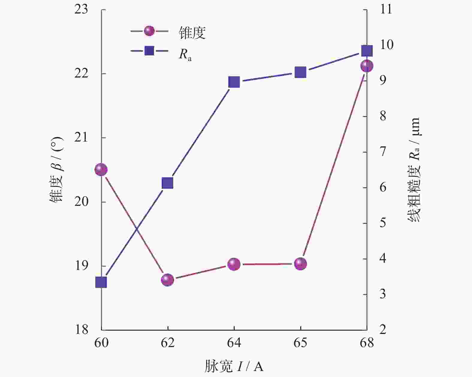
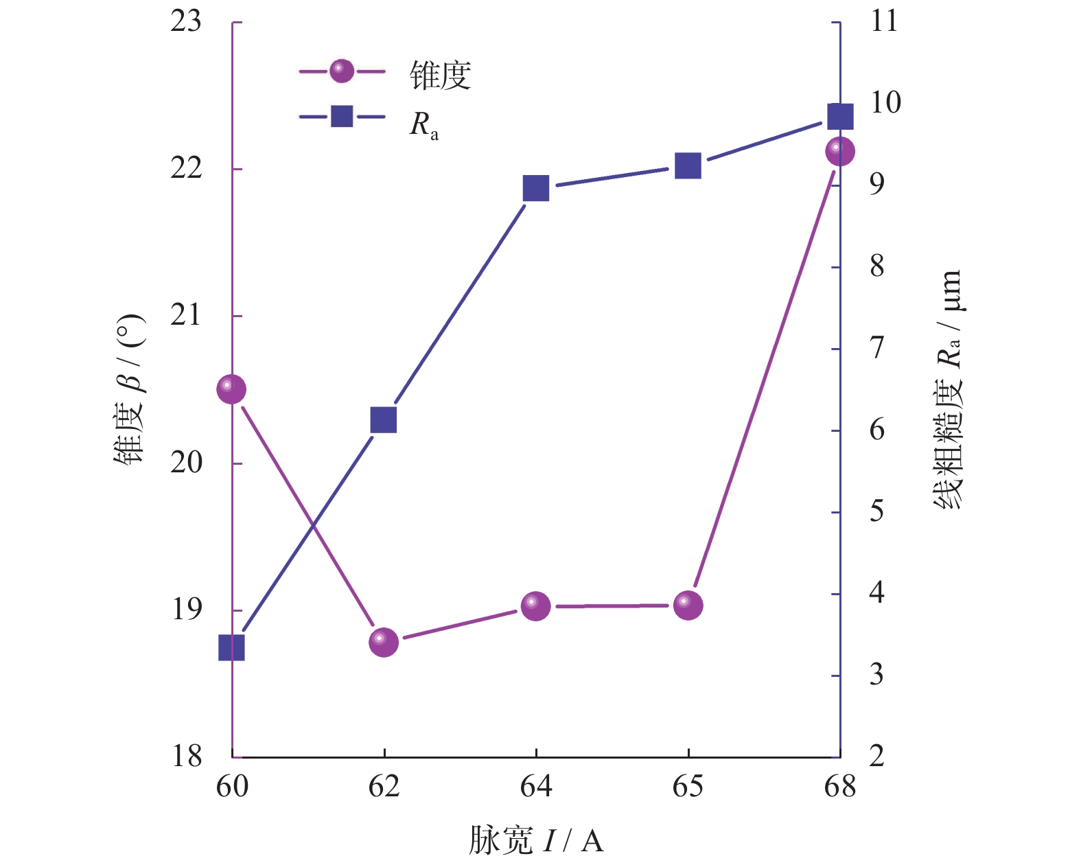
图 5 切缝锥度和线粗糙度Ra随激光电流变化曲线
Figure 5. Curves of taper and roughness Ra changing with current
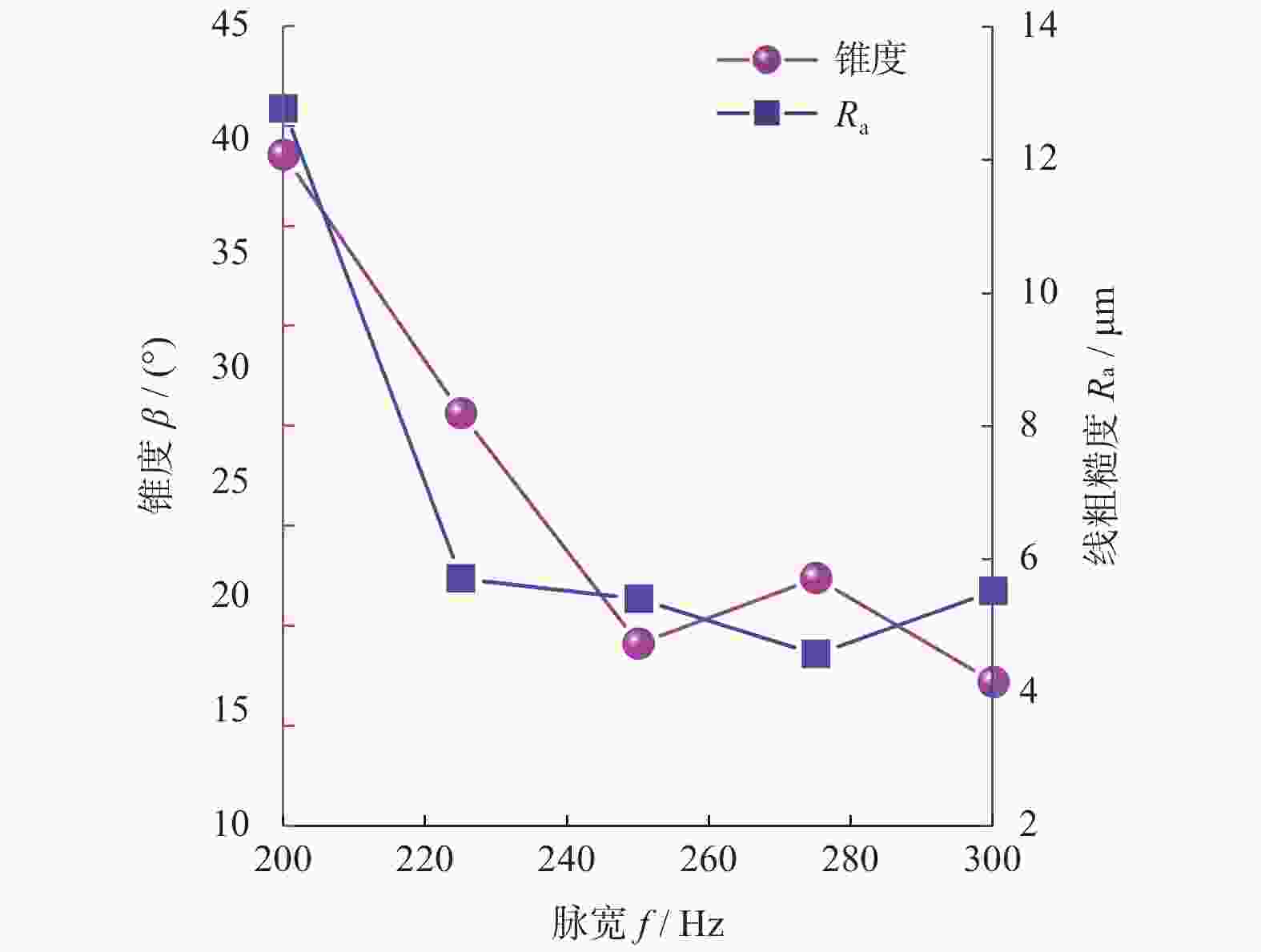
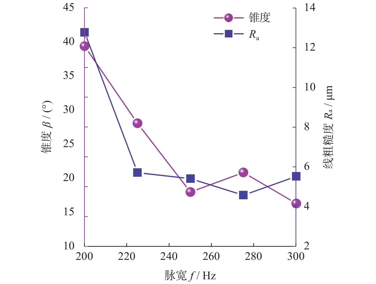
图 6 切缝锥度和线粗糙度Ra随频率变化曲线影响
Figure 6. Curves of taper and roughness Ra changing with frequency

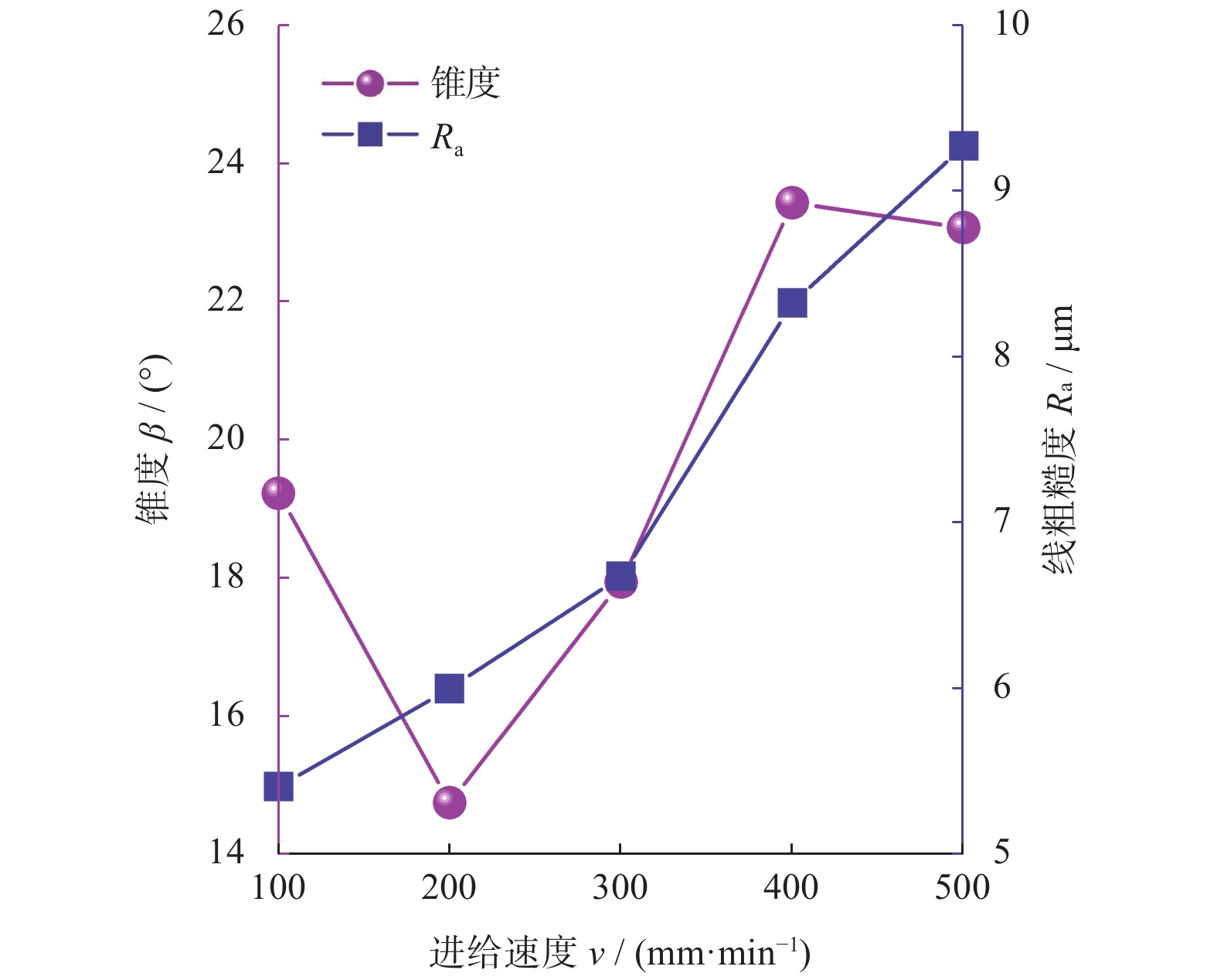
图 7 切缝锥度和线粗糙度Ra随进给速度变化曲线
Figure 7. Curves of taper and roughness Ra changing with feed speed

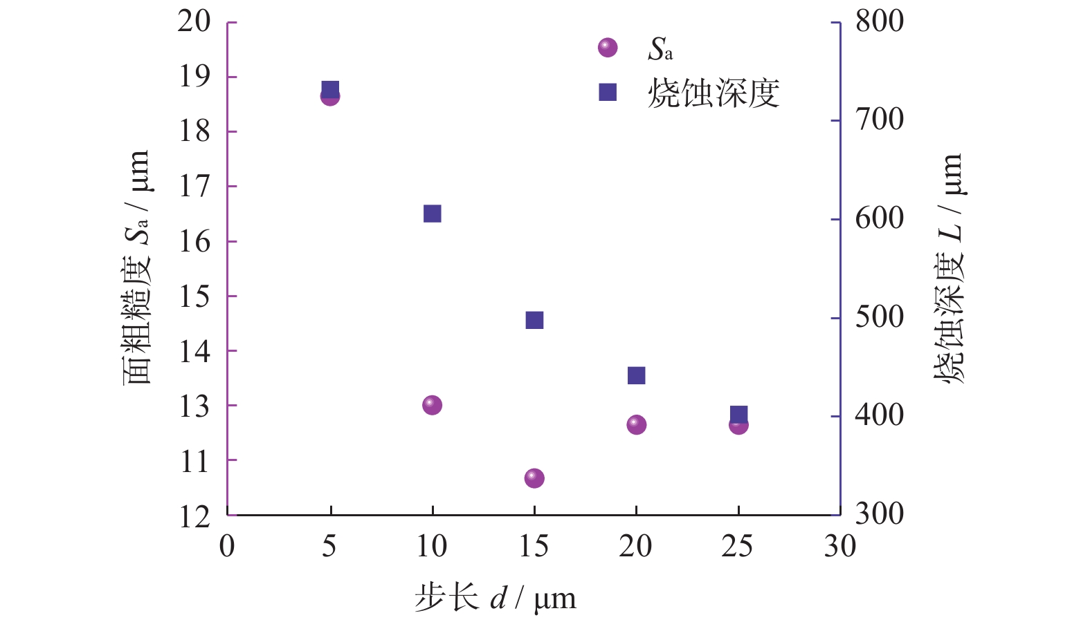
图 8 面粗糙度Sa和烧蚀深度随切缝步长变化曲线
Figure 8. Variations of surface roughness Sa and ablation depth with step size
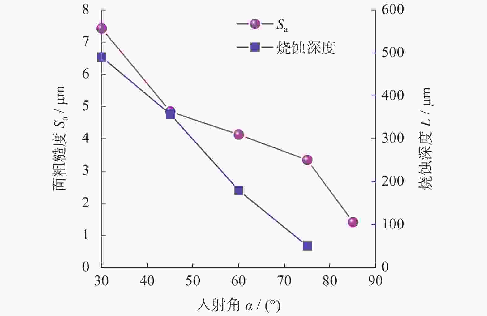
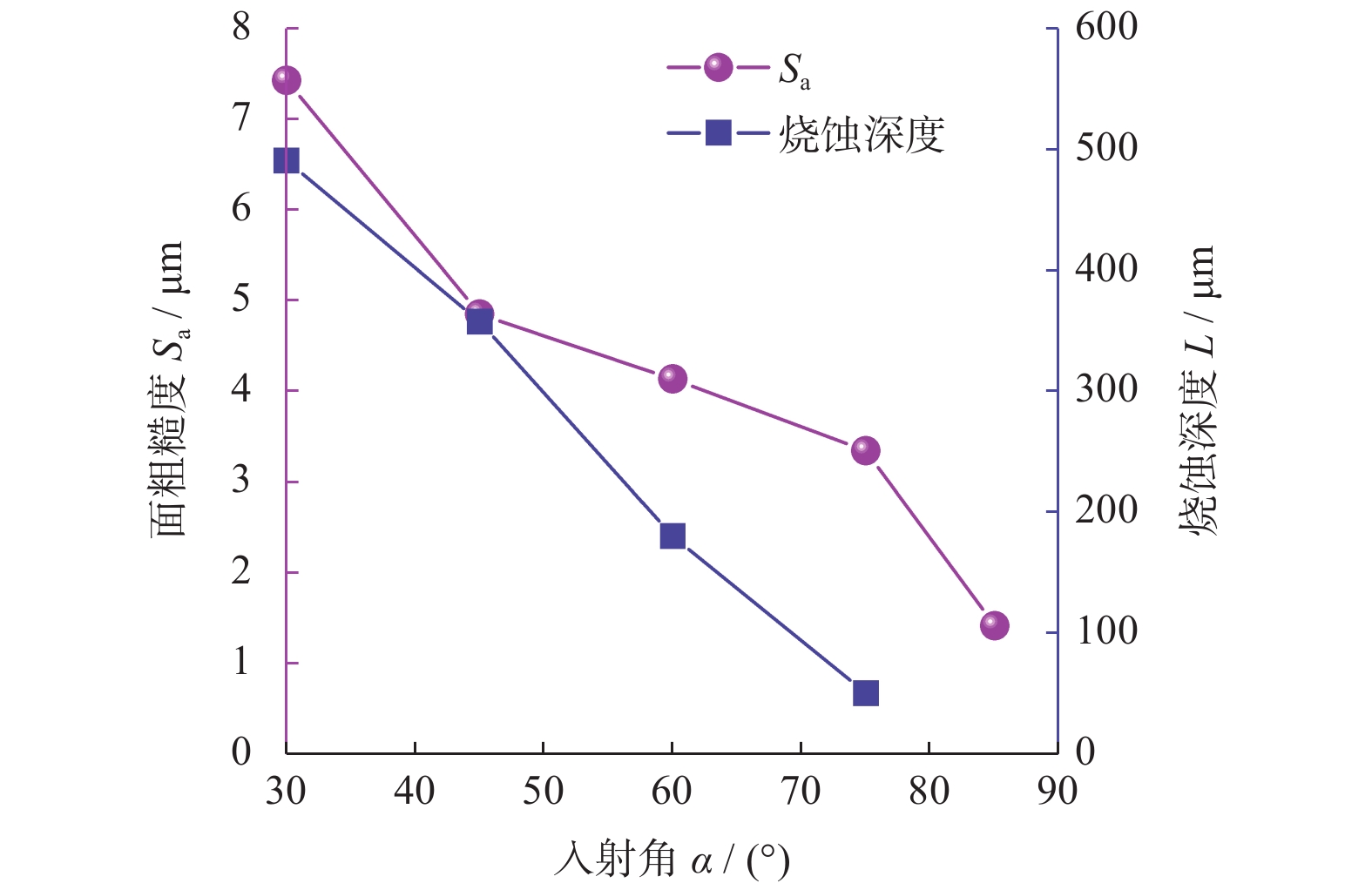
图 10 面粗糙度Sa和烧蚀深度随入射角α变化曲线
Figure 10. Curves of surface roughness Sa and ablation depth changing with incident angle
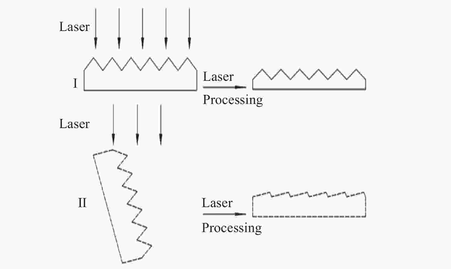
图 11 激光平整金刚石膜表面原理图
Figure 11. Schematic diagram of laser flattening diamond film surface
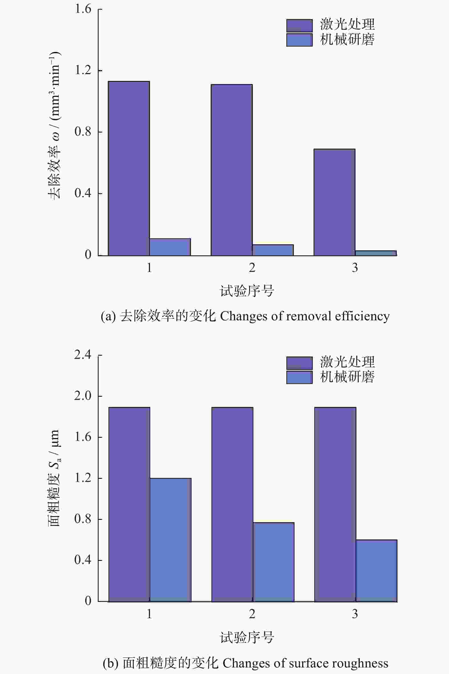
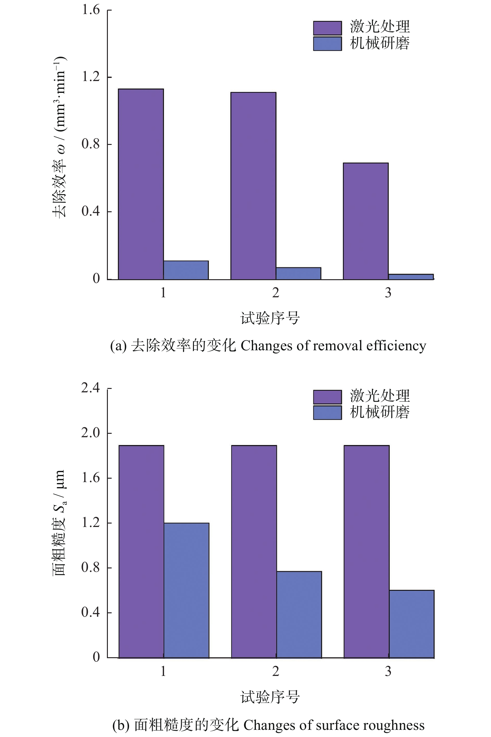
图 12 3组试验的材料去除效率和面粗糙度Sa变化
Figure 12. Changes of material removal efficiency and surface roughness Sa in three groups of experiments
表 1 正交试验工艺参数
Table 1. Orthogonal test process parameters
水平 A
电流 I / AB
脉宽 t / μsC
频率 f / HzD
进给速度 v / (mm·min−1)1 60 400 200 100 2 62 425 225 200 3 64 450 250 300 4 66 475 275 400 5 68 500 300 500  下载: 导出CSV
表 2 机械研磨和激光平整化对比参数
Table 2. Comparative parameters of mechanical grinding and laser planarization
试验序号 粒度代号 进给速度 v / (mm·min−1) 1 80/100 100 2 200/230 200 3 M36/54 300
下载: 导出CSV
-
[1] AN K, CHEN L X, YAN X B, et al. Fracture strength and toughness of chemical-vapor-deposited polycrystalline diamond films [J]. Ceramics International,2018,44(15):17845-17851. doi: 10.1016/j.ceramint.2018.06.253 [2] 刘金龙, 安康, 陈良贤, 等. CVD金刚石自支撑膜的研究进展 [J]. 表面技术,2018,47(4):1-10.LIU Jinlong, AN Kang, CHEN Liangxian, et al. Research progress of freestanding CVD diamond films [J]. Surface Technology,2018,47(4):1-10. [3] GRUEN D M, BUCKLEY-GOLDER I. Diamond films: Recent developments [J]. MRS Bulletin,2013,23(9):16-21. [4] SCHWANDER M, PARTES K. A review of diamond synthesis by CVD processes [J]. Diamond and Related Materials,2011,20(9):1287-1301. doi: 10.1016/j.diamond.2011.08.005 [5] KHAN B A, LITVINYUK I V, RYBACHUK M. Femtosecond laser micromachining of diamond: Current research status, applications and challenges [J]. Carbon,2021,179:209-226. doi: 10.1016/j.carbon.2021.04.025 [6] ZHENG Y T, LI C M, LIU J L, et al. Diamond with nitrogen: States, control, and applications [J]. Functional Diamond,2021,1(1):63-82. doi: 10.1080/26941112.2021.1877021 [7] SAKAUCHI K, NAGAI M, TABAKOYA T, et al. Mechanical damage-free surface planarization of single-crystal diamond based on carbon solid solution into nickel [J]. Diamond and Related Materials,2021,116:1-6. [8] MAN W D, WANG J H, WANG C X, et al. Planarizing CVD diamond films by using hydrogen plasma etching enhanced carbon diffusion process [J]. Diamond and Related Materials,2007,16(8):1455-1458. doi: 10.1016/j.diamond.2006.11.102 [9] ILIAS S, SENE G, MOLLER P, et al. Planarization of diamond thin film surfaces by ion beam etching at grazing incidence angle [J]. Diamond and Related Materials,1996,5(6/7/8):835-839. doi: 10.1016/0925-9635(95)00412-2 [10] NORIKAZU S, MISONO H, SHAMOTO E, et al. Material removal efficiency improvement by orientation control of CMP pad surface asperities [J]. Precision Engineering,2020,62:83-88. doi: 10.1016/j.precisioneng.2019.11.008 [11] 徐峰. CVD金刚石厚膜的加工技术研究 [D]. 南京: 南京航空航天大学, 2002.XU Feng. Study on laser processing and machining of CVD diamond thick-film [D]. Nanjing: Nanjing University of Aeronautics and Astronautics, 2002. [12] 季国顺, 张永康. 激光抛光化学气相沉积金刚石膜 [J]. 激光技术,2003,27(2):106-109. doi: 10.3969/j.issn.1001-3806.2003.02.005JI Guoshun, ZHANG Yongkang. Laser polishing of chemically vapor-deposited diamond films [J]. Laser Technology,2003,27(2):106-109. doi: 10.3969/j.issn.1001-3806.2003.02.005 [13] 安康. 等离子体喷射金刚石膜板力学性能基础研 [D]. 北京: 北京科技大学, 2019.AN Kang. Basic research on mechanical properties of thick diamond film fabricated by plasma jet CVD [D]. Beijing: University of Science and Technology Beijing, 2019. [14] AN K, CHEN L X, YAN X B, et al. Fracture behavior of diamond films deposited by DC arc plasma jet CVD [J]. Ceramics International,2018, 44(11):13402-13408. [15] 刘立君, 王晓陆, 沈秀强, 等. 耐热钢表面激光熔覆陶瓷工艺 [J]. 哈尔滨理工大学学报,2020,25(1):7.Liu Lijun, Wang Xiaolu, Shen Xiuqiang, et al. Technology of laser cladding ceramics on heat resistant steel surface [J]. Journal of Harbin University of Science and Technology,2020,25(1):7. [16] LI C M, ZHU R H, LIU J L, et al. Effect of arc characteristics on the properties of large size diamond wafer prepared by DC arc plasma jet CVD [J]. Diamond and Related Materials,2013,39(10):47-52. [17] QI Z N, ZHENG Y T, WEI J J, et al. Surface treatment of an applied novel all-diamond microchannel heat sink for heat transfer performance enhancement [J]. Applied Thermal Engineering,2020,177:1-13. [18] TSAI H Y, TING C J, CHOU C P. Evaluation research of polishing methods for large area diamond films produced by chemical vapor deposition [J]. Diamond and Related Materials,2007,16(2):253-261. doi: 10.1016/j.diamond.2006.06.007 -


 点击查看大图
计量
- 文章访问数: 947
- HTML全文浏览量: 338
- PDF下载量: 90
- 被引次数: 0
 邮件订阅
邮件订阅 RSS
RSS