CN 41-1243/TG
ISSN 1006-852X
| Citation: | LIU Fucheng, MA Guanjie, HUANG Jiangtao, ZHANG Zongyan, HAN Peigang, HE Bin. Advances in studies and applications of thick diamond films prepared by microwave plasma chemical vapor deposition[J]. Diamond & Abrasives Engineering, 2025, 45(3): 285-299. doi: 10.13394/j.cnki.jgszz.2023.0270

|

| [1] |
林晓棋, 满卫东, 张玮, 等. MPCVD法合成大单晶金刚石的研究进展 [J]. 硬质合金,2013,30(5):288-296.
LIN Xiaoqi, MAN Weidong, ZHANG Wei, et al. Research progress on synthesis of large-scale single crystal diamond by MPCVD [J]. Cemented Carbide,2013,30(5):288-296.
|
| [2] |
SCHRECK M, GSELL S, BRESCIA R, et al. Ion bombardment induced buried lateral growth: The key mechanism for the synthesis of single crystal diamond wafers [J]. Scientific Reports,2017,7:44462. doi: 10.1038/srep44462
|
| [3] |
吕反修. 金刚石膜制备与应用:下卷 [M]. 北京: 科学出版社, 2014.
LYU Fanxiu. Preparation and application of diamond film: Volume 2 [M]. Beijing: Science Press, 2014.
|
| [4] |
BUNDY F P, HALL H T, STRONG H M, et al. Man-made diamonds [J]. Nature,1955,176(4471):51-55. doi: 10.1038/176051a0
|
| [5] |
ANGUS J C, WILL H A, STANKO W S. Growth of diamond seed crystals by vapor deposition [J]. Journal of Applied Physics, 1968, 39(6): 2915-2922. doi: 10.1063/1.1656693
|
| [6] |
GORDON M H, DUTEN X, HASSOUNI K, et al. Energy coupling efficiency of a hydrogen microwave plasma reactor [J]. Journal of Applied Physics, 2001, 89(3): 1544-1549. doi: 10.1063/1.1337593
|
| [7] |
VIKHAREV A L, GORBACHEV A M, KOZLOV A V, et al. Microcrystalline diamond growth in presence of argon in millimeter-wave plasma-assisted CVD reactor [J]. Diamond and Related Materials,2008,17(7/8/9/10):1055-1061. doi: 10.1016/j.diamond.2008.01.050
|
| [8] |
YAMAMOTO M, TERAJI T, ITO T. Improvement in the crystalline quality of homoepitaxial diamond films by oxygen plasma etching of mirror-polished diamond substrates [J]. Journal of Crystal Growth,2005,285(1/2):130-136. doi: 10.1016/j.jcrysgro.2005.08.019
|
| [9] |
LIN C R, LIAO W H, WEI D H, et al. Fabrication of highly transparent ultrananocrystalline diamond films from focused microwave plasma jets [J]. Surface and Coatings Technology,2013,231:594-598. doi: 10.1016/j.surfcoat.2012.01.052
|
| [10] |
FENDRYCH F, TAYLOR A, PEKSA L, et al. Growth and characterization of nanodiamond layers prepared using the plasma-enhanced linear antennas microwave CVD system [J]. Journal of Physics D: Applied Physics,2010,43(37):374018. doi: 10.1088/0022-3727/43/37/374018
|
| [11] |
刘金龙, 安康, 陈良贤, 等. CVD金刚石自支撑膜的研究进展 [J]. 表面技术,2018,47(4):1-10. doi: 10.16490/j.cnki.issn.1001-3660.2018.04.001
LIU Jinlong, AN Kang, CHEN Liangxian, et al. Research progress of free-standing CVD diamond films [J]. Surface Technology,2018,47(4):1-10. doi: 10.16490/j.cnki.issn.1001-3660.2018.04.001
|
| [12] |
ASKARI S J, CHEN G C, LU F X. Growth of polycrystalline and nanocrystalline diamond films on pure titanium by microwave plasma assisted CVD process [J]. Materials Research Bulletin,2008,43(5):1086-1092. doi: 10.1016/j.materresbull.2007.06.010
|
| [13] |
SU J J, LI Y F, LI X L, et al. A novel microwave plasma reactor with a unique structure for chemical vapor deposition of diamond films [J]. Diamond and Related Materials,2014,42:28-32. doi: 10.1016/j.diamond.2013.12.001
|
| [14] |
李义锋. 新型高功率MPCVD装置研制与金刚石膜高效沉积 [D]. 北京: 北京科技大学, 2015.
LI Yifeng. Development of a new high power MPCVD device and efficient deposition of diamond films [D]. Beijing: University of Science and Technology Beijing, 2015.
|
| [15] |
李义锋, 唐伟忠, 姜龙, 等. 915MHz高功率MPCVD装置制备大面积高品质金刚石膜 [J]. 人工晶体学报,2019,48(7):1262-1267. doi: 10.3969/j.issn.1000-985X.2019.07.013
LI Yifeng, TANG Weizhong, JIANG Long, et al. Large area high quality diamond films deposition by 915 MHz high power MPCVD reactor [J]. Journal of Synthetic Crystals,2019,48(7):1262-1267. doi: 10.3969/j.issn.1000-985X.2019.07.013
|
| [16] |
佚名. 微波等离子体化学气相沉积系统简介及研发进展[EB/OL]. (2020-07-10)[2023-07-13]. http://www.xdwh-inst.com/display/349355.html.
Anonymous. Introduction and development progress of microwave plasma chemical vapor deposition system[EB/OL]. (2020-07-10)[2023-07-13]. http://www.xdwh-inst.com/display/349355.html.
|
| [17] |
SHIH H C, SUNG C P, TANG Y S, et al. Microstructure and characterization of diamond film grown on various substrates [J]. Surface and Coatings Technology,1992,52(2):105-114. doi: 10.1016/0257-8972(92)90034-8
|
| [18] |
SEDOV V, MARTYANOV A, ALTAKHOV A, et al. Effect of substrate holder design on stress and uniformity of large-area polycrystalline diamond films grown by microwave plasma-assisted CVD [J]. Coatings,2020,10(10):939. doi: 10.3390/coatings10100939
|
| [19] |
BOLSHAKOV A P, RALCHENKO V G, YUROV V Y, et al. Enhanced deposition rate of polycrystalline CVD diamond at high microwave power densities [J]. Diamond and Related Materials,2019,97:107466. doi: 10.1016/j.diamond.2019.107466
|
| [20] |
MITSUDA Y, KOJIMA Y, YOSHIDA T, et al. The growth of diamond in microwave plasma under low pressure [J]. Journal of Materials Science,1987,22(5):1557-1562. doi: 10.1007/BF01132374
|
| [21] |
张青, 翁俊, 刘繁, 等. 高功率微波等离子体对单晶金刚石同质外延生长的影响 [J]. 表面技术,2022,51(6):364-373,398. doi: 10.16490/j.cnki.issn.1001-3660.2022.06.035
ZHANG Qing, WENG Jun, LIU Fan, et al. Effect of high microwave power plasma on the homogeneous epitaxy growth of single crystal diamond [J]. Surface Technology,2022,51(6):364-373,398. doi: 10.16490/j.cnki.issn.1001-3660.2022.06.035
|
| [22] |
MANDAL S. Nucleation of diamond films on heterogeneous substrates: A review [J]. RSC Advances,2021,11(17):10159-10182. doi: 10.1039/D1RA00397F
|
| [23] |
TANG C J, FERNANDES A J S, JIANG X F, et al. Effect of methane concentration in hydrogen plasma on hydrogen impurity incorporation in thick large-grained polycrystalline diamond films [J]. Journal of Crystal Growth,2015,426:221-227. doi: 10.1016/j.jcrysgro.2015.06.018
|
| [24] |
罗凯, 汪建华, 余军火, 等. 高功率微波等离子体环境下甲烷浓度对金刚石膜的影响 [J]. 化工学报,2018,69(S2):505-511. doi: 10.11949/j.issn.0438-1157.20181169
LUO Kai, WANG Jianhua, YU Junhuo, et al. Effect of methane concentration on diamond film in high power microwave plasma environment [J]. CIESC Journal,2018,69(S2):505-511. doi: 10.11949/j.issn.0438-1157.20181169
|
| [25] |
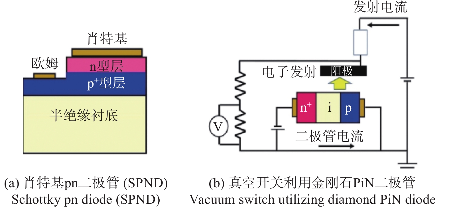
MÜLLER-SEBERT W, WÖRNER E, FUCHS F, et al. Nitrogen induced increase of growth rate in chemical vapor deposition of diamond [J]. Applied Physics Letters,1996,68(6):759-760. doi: 10.1063/1.116733
|
| [26] |
SEDOV V, MARTYANOV A, SAVIN S, et al. CVD synthesis of multi-layered polycrystalline diamond films with reduced roughness using time-limited injections of N2 gas [J]. Diamond and Related Materials,2021,114:108333. doi: 10.1016/j.diamond.2021.108333
|
| [27] |
王蒙, 翁俊, 刘繁, 等. 氩气对高功率MPCVD制备金刚石膜的影响 [J]. 化学工程与装备,2021(10):5-6. doi: 10.19566/j.cnki.cn35-1285/tq.2021.10.003
WANG Meng, WENG Jun, LIU Fan, et al. Effect of argon on diamond films prepared by high power MPCVD [J]. Chemical Engineering & Equipment,2021(10):5-6. doi: 10.19566/j.cnki.cn35-1285/tq.2021.10.003
|
| [28] |
CHEIN T H, WEI J, TZENG Y. Synthesis of diamond in high power-density microwave methane/hydrogen/oxygen plasmas at elevated substrate temperatures [J]. Diamond and Related Materials,1999,8(8/9):1686-1696. doi: 10.1016/S0925-9635(99)00059-X
|
| [29] |
ANDO Y, YOKOTA Y, TACHIBANA T, et al. Large area deposition of 〈100〉-textured diamond films by a 60-kW microwave plasma CVD reactor [J]. Diamond and Related Materials,2002,11(3/4/5/6):596-600. doi: 10.1016/S0925-9635(02)00018-3
|
| [30] |
HEMAWAN K W, GROTJOHN T A, REINHARD D K, et al. Improved microwave plasma cavity reactor for diamond synthesis at high-pressure and high power density [J]. Diamond and Related Materials,2010,19(12):1446-1452. doi: 10.1016/j.diamond.2010.07.005
|
| [31] |
KAMO M, SATO Y, MATSUMOTO S, et al. Diamond synthesis from gas phase in microwave plasma [J]. Journal of Crystal Growth,1983,62(3):642-644. doi: 10.1016/0022-0248(83)90411-6
|
| [32] |
RALCHENKO V G, SAVELIEV A V, POPOVICH A F, et al. CVD diamond coating of AlN ceramic substrates to enhance heat removal [J]. Russian Microelectronics,2006,35(4):205-209. doi: 10.1134/S1063739706040019
|
| [33] |
VIKHAREV A L, GORBACHEV A M, LOBAEV M A, et al. Multimode cavity type MPACVD reactor for large area diamond film deposition [J]. Diamond and Related Materials,2018,83:8-14. doi: 10.1016/j.diamond.2018.01.011
|
| [34] |
HONG S P, LEE K I, YOU H J, et al. Scanning deposition method for large-area diamond film synthesis using multiple microwave plasma sources [J]. Nanomaterials,2022,12(12):1959. doi: 10.3390/nano12121959
|
| [35] |
RIFAI A, CREEDON D, TRAN N, et al. Highly uniform polycrystalline diamond coatings of three-dimensional structures [J]. Surface and Coatings Technology,2021,408:126815. doi: 10.1016/j.surfcoat.2020.126815
|
| [36] |
FÜNER M, WILD C, KOIDL P. Simulation and development of optimized microwave plasma reactors for diamond deposition [J]. Surface and Coatings Technology,1999,116:853-862. doi: 10.1016/S0257-8972(99)00233-9
|
| [37] |
YAMADA H, CHAYAHARA A, UMEZAWA H, et al. Fabrication and fundamental characterizations of tiled clones of single-crystal diamond with 1-inch size [J]. Diamond and Related Materials,2012,24:29-33. doi: 10.1016/j.diamond.2011.09.007
|
| [38] |
YAMADA H, CHAYAHARA A, MOKUNO Y, et al. Uniform growth and repeatable fabrication of inch-sized wafers of a single-crystal diamond [J]. Diamond and Related Materials,2013,33:27-31. doi: 10.1016/j.diamond.2012.12.012
|
| [39] |
YAMADA H, CHAYAHARA A, MOKUNO Y, et al. A 2-in. mosaic wafer made of a single-crystal diamond [J]. Applied Physics Letters, 14, 104(10): 102110.
|
| [40] |
佚名. 金刚石半导体越来越近[EB/OL]. (2022-04-04)[2024-04-15]. https://baijiahao.baidu.com/s?id=1762216523971146798&wfr=spider&for=pc.
Anonymous. Diamond semiconductors are getting closer and closer [EB/OL]. (2022-04-04)[2024-04-15]. https://baijiahao.baidu.com/s?id=1762216523971146798&wfr=spider&for=pc.
|
| [41] |
DT半导体材料. 全球首个!100 mm的金刚石晶圆面世 [EB/OL]. (2023-1-08)[2024-04-16]. https://www.eet-china.com/mp/a264952.html
DT semiconductor material. World’s first diamond wafer [EB/OL]. (2023-1-08)[2024-04-16]. https://www.eet-china.com/mp/a264952.html.
|
| [42] |
SU J J, LI Y F, DING M H, et al. A dome-shaped cavity type microwave plasma chemical vapor deposition reactor for diamond films deposition [J]. Vacuum,2014,107:51-55.
|
| [43] |
LI X J, TANG W Z, YU S W, et al. Design of novel plasma reactor for diamond film deposition [J]. Diamond and Related Materials,2011,20(4):480-484. doi: 10.1016/j.diamond.2011.01.046
|
| [44] |
LI Y F, SU J J, LIU Y Q, et al. Design of a new TM021 mode cavity type MPCVD reactor for diamond film deposition [J]. Diamond and Related Materials,2014,44:88-94. doi: 10.1016/j.diamond.2014.02.010
|
| [45] |
LI Y F, AN X M, LIU X C, et al. A 915MHz/75kW cylindrical cavity type microwave plasma chemical vapor deposition reactor with a ladder-shaped circumferential antenna developed for growing large area diamond films [J]. Diamond and Related Materials,2017,78:67-72. doi: 10.1016/j.diamond.2017.08.007
|
| [46] |
张帅, 安康, 杨志亮, 等. 新型MPCVD沉积模式制备高均匀性的D100 mm金刚石薄膜 [J]. 真空与低温,2022,28(5):549-555. doi: 10.3969/j.issn.1006-7086.2022.05.008
ZHANG Shuai, AN Kang, YANG Zhiliang, et al. 100 mm in diameter diamond films with high uniformity prepared by novel deposition mode in MPCVD system [J]. Vacuum and Cryogenics,2022,28(5):549-555. doi: 10.3969/j.issn.1006-7086.2022.05.008
|
| [47] |
于盛旺, 安康, 李晓静, 等. 高功率MPCVD金刚石膜红外光学材料制备 [J]. 红外与激光工程,2013,42(4):971-974. doi: 10.3969/j.issn.1007-2276.2013.04.025
YU Shengwang, AN Kang, LI Xiaojing, et al. Preparation of diamond films as an infrared optical material by high power microwave plasma CVD [J]. Infrared and Laser Engineering,2013,42(4):971-974. doi: 10.3969/j.issn.1007-2276.2013.04.025
|
| [48] |
于盛旺, 刘艳青, 唐伟忠, 等. 高功率MPCVD金刚石膜透波窗口材料制备研究 [J]. 人工晶体学报,2012,41(4):896-899. doi: 10.3969/j.issn.1000-985X.2012.04.014
YU Shengwang, LIU Yanqing, TANG Weizhong, et al. Synthesis of diamond film as electromagnetic window material by an ellipsoidal MPCVD reactor at high input microwave power levels [J]. Journal of Synthetic Crystals,2012,41(4):896-899. doi: 10.3969/j.issn.1000-985X.2012.04.014
|
| [49] |
YU S W, WANG R, ZHENG K, et al. Influence of power density on high purity 63 mm diameter polycrystalline diamond deposition inside a 2.45 GHz MPCVD reactor [J]. Journal of Physics D: Applied Physics,2016,49(35):355202. doi: 10.1088/0022-3727/49/35/355202
|
| [50] |
LI X J, ZHOU S, CHEN G, et al. Systematic research on the performance of self-designed microwave plasma reactor for CVD high quality diamond [J]. Defence Technology,2018,14(5):373-379. doi: 10.1016/j.dt.2018.05.004
|
| [51] |
杨国永, 熊绍阳, 鲁云祥, 等. 大尺寸自支撑金刚石膜制备工艺及其红外透过性能研究 [J]. 硬质合金,2020,37(5):350-356. doi: 10.3969/j.issn.1003-7292.2020.05.004
YANG Guoyong, XIONG Shaoyang, LU Yunxiang, et al. Study of large-area free-standing diamond films and its property of infrared transmittance [J]. Cemented Carbide,2020,37(5):350-356. doi: 10.3969/j.issn.1003-7292.2020.05.004
|
| [52] |
佚名. 郑州大学研制出两英寸光学级金刚石晶体[EB/OL]. (2019-09-26)[2023-07-14]. https://www.nsfc.gov.cn/csc/20340/20289/45388/index.html.
Anonymous. Zhengzhou University has developed two inch optical grade diamond crystals [EB/OL]. (2019-09-26)[2023-07-14]. https://www.nsfc.gov.cn/csc/20340/20289/45388/index.html.
|
| [53] |
梁天, 汪建华, 翁俊, 等. 高气压对MPCVD沉积金刚石薄膜的影响 [J]. 真空与低温,2018,24(1):54-59. doi: 10.3969/j.issn.1006-7086.2018.01.010
LIANG Tian, WANG Jianhua, WENG Jun, et al. Influence of high pressure on MPCVD deposition of diamond films [J]. Vacuum and Cryogenics,2018,24(1):54-59. doi: 10.3969/j.issn.1006-7086.2018.01.010
|
| [54] |
丁康俊, 马志斌, 宋修曦, 等. 温度对MPCVD法同质外延单晶金刚石缺陷的影响 [J]. 金刚石与磨料磨具工程,2018,38(2):8-11,19. doi: 10.13394/j.cnkij.gszz.2018.2.0002
DING Kangjun, MA Zhibin, SONG Xiuxi, et al. Effect of temperature on defects in homoepitaxial single crystal diamond by MPCVD [J]. Diamond & Abrasives Engineering,2018,38(2):8-11,19. doi: 10.13394/j.cnkij.gszz.2018.2.0002
|
| [55] |
夏禹豪, 李艳春, 耿传文, 等. MPCVD中双基片台结构对单晶金刚石生长的影响 [J]. 金刚石与磨料磨具工程,2018,38(3):1-5. doi: 10.13394/j.cnki.jgszz.2018.3.0001
XIA Yuhao, LI Yanchun, GENG Chuanwen, et al. Influence of dual-substrate structure on growth of single crystal diamond by MPCVD [J]. Diamond & Abrasives Engineering,2018,38(3):1-5. doi: 10.13394/j.cnki.jgszz.2018.3.0001
|
| [56] |
夏禹豪, 耿传文, 衡凡, 等. MPCVD法中氮气对单晶金刚石生长机理影响的探究 [J]. 真空科学与技术学报,2018,38(8):684-688. doi: 10.13922/j.cnki.cjovst.2018.08.07
XIA Yuhao, GENG Chuanwen, HENG Fan, et al. Impact of nitrogen concentration on monocrystalline diamond growth in microwave plasma chemical vapor deposition [J]. Chinese Journal of Vacuum Science and Technology,2018,38(8):684-688. doi: 10.13922/j.cnki.cjovst.2018.08.07
|
| [57] |
王斌, 汪建华, 翁俊, 等. 气体流动方式对MPCVD金刚石薄膜均匀性的影响 [J]. 真空与低温,2020,26(2):108-113. doi: 10.3969/j.issn.1006-7086.2020.02.004
WANG Bin, WANG Jianhua, WENG Jun, et al. Effect of gas flow mode on uniformity of MPCVD diamond films [J]. Vacuum and Cryogenics,2020,26(2):108-113. doi: 10.3969/j.issn.1006-7086.2020.02.004
|
| [58] |
何中文, 马志斌. 高等离子体功率密度下MPCVD法制备多晶金刚石膜 [J]. 金刚石与磨料磨具工程,2022,42(2):156-161. doi: 10.13394/J.cnki.jgszz.2021.0121
HE Zhongwen, MA Zhibin. Preparation of polycrystalline diamond films by MPCVD at high plasma power density [J]. Diamond & Abrasives Engineering,2022,42(2):156-161. doi: 10.13394/J.cnki.jgszz.2021.0121
|
| [59] |
WANG Q J, WU G, LIU S, et al. Simulation-based development of a new cylindrical-cavity microwave-plasma reactor for diamond-film synthesis [J]. Crystals,2019,9(6):320. doi: 10.3390/cryst9060320
|
| [60] |
YANG B, SHEN Q, GAN Z Y, et al. Analysis of improving the edge quality and growth rate of single-crystal diamond growth using a substrate holder [J]. CrystEngComm,2019,21(43):6574-6584. doi: 10.1039/C9CE01402K
|
| [61] |
BANERJEE A, BERNOULLI D, ZHANG H T, et al. Ultralarge elastic de-formation of nanoscale diamond [J]. Science,2018,360(6386):300-302. doi: 10.1126/science.aar4165
|
| [62] |
陈良贤, 刘金龙, 冯寅楠, 等. 金刚石上不同晶体结构Y2O3膜性质与增透性能研究 [J]. 表面技术,2019,48(1):133-140. doi: 10.16490/j.cnki.issn.1001-3660.2019.01.017
CHEN Liangxian, LIU Jinlong, FENG Yinnan, et al. Properties and anti-reflection performance of Y2O3 films with different crystal structures on diamond [J]. Surface Technology,2019,48(1):133-140. doi: 10.16490/j.cnki.issn.1001-3660.2019.01.017
|
| [63] |
左杨平, 卢文壮, 张圣斌, 等. 面向激光防护应用的金刚石/V2O5膜系设计与制备 [J]. 红外与激光工程,2015,44(8):2491-2495. doi: 10.3969/j.issn.1007-2276.2015.08.042
ZUO Yangping, LU Wenzhuang, ZHANG Shengbin, et al. Design and fabrication of diamond/V2O5 films in continuous laser protection [J]. Infrared and Laser Engineering,2015,44(8):2491-2495. doi: 10.3969/j.issn.1007-2276.2015.08.042
|
| [64] |
吕反修, 高旭辉, 郭会斌, 等. 在预涂陶瓷过渡层的多谱段ZnS衬底上沉积金刚石膜的探索研究 [J]. 人工晶体学报,2004,33(1):105-108. doi: 10.3969/j.issn.1000-985X.2004.01.023
LYU Fanxiu, GAO Xuhui, GUO Huibin, et al. An exploratory study on preparation of diamond film coatings on multi-spectra ZnS pre-coated with a ceramic interlayer [J]. Journal of Synthetic Crystals,2004,33(1):105-108. doi: 10.3969/j.issn.1000-985X.2004.01.023
|
| [65] |
黄亚博, 陈良贤, 贾鑫, 等. CVD金刚石表面增透膜的研究进展 [J]. 表面技术,2020,49(10):106-117. doi: 10.16490/j.cnki.issn.1001-3660.2020.10.012
HUANG Yabo, CHEN Liangxian, JIA Xin, et al. Research progress of anti-reflection films on CVD diamond surface [J]. Surface Technology,2020,49(10):106-117. doi: 10.16490/j.cnki.issn.1001-3660.2020.10.012
|
| [66] |
白振旭, 杨学宗, 陈晖, 等. 高功率金刚石激光技术研究进展(特邀) [J]. 红外与激光工程,2020,49(12):9-21. doi: 10.3788/IRLA20201076
BAI Zhenxu, YANG Xuezong, CHEN Hui, et al. Research progress of high-power diamond laser technology(Invited) [J]. Infrared and Laser Engineering,2020,49(12):9-21. doi: 10.3788/IRLA20201076
|
| [67] |
王伟华, 代兵, 王杨, 等. 金刚石光学窗口相关元件的研究进展 [J]. 材料科学与工艺,2020,28(3):42-57. doi: 10.11951/j.issn.1005-0299.20200074
WANG Weihua, DAI Bing, WANG Yang, et al. Recent progress of diamond optical window-related components [J]. Materials Science and Technology,2020,28(3):42-57. doi: 10.11951/j.issn.1005-0299.20200074
|
| [68] |
Optics: Enable extreme performance photonics [EB/OL]. [2021-07-14]. https://www.e6.com/en/knowledge-base/brochures.
|
| [69] |
李凤凤, 刘永佳, 张建华. 培育钻石的发展现状及应用研究 [J]. 超硬材料工程,2022,34(4):51-54. doi: 10.3969/j.issn.1673-1433.2022.04.011
LI Fengfeng, LIU Yongjia, ZHANG Jianhua. Development status and application of diamond cultivation [J]. Superhard Material Engineering,2022,34(4):51-54. doi: 10.3969/j.issn.1673-1433.2022.04.011
|
| [70] |
王光祖, 位星, 张相法, 等. 饰钻培育技术的由来与兴起 [J]. 超硬材料工程,2022,34(5):42-47. doi: 10.3969/j.issn.1673-1433.2022.05.010
WANG Guangzu, WEI Xing, ZHANG Xiangfa, et al. Origin and rise of decorative diamond cultivation technology [J]. Superhard Material Engineering,2022,34(5):42-47. doi: 10.3969/j.issn.1673-1433.2022.05.010
|
| [71] |
佚名. GIA鉴定34.59克拉化学气相沉积法(CVD)实验室培育钻石 [EB/OL]. (2023-05-29)[2023-07-14]. https://baijiahao.baidu.com/s?id=1767205622858628324&wfr=spider&for=pc.
Anonymous. GIA Identification 34.59 Carat Chemical Vapor Deposition (CVD) Laboratory Cultivated Diamond [EB/OL]. (2023-05-29)[2023-07-14]. https://baijiahao.baidu.com/s?id=1767205622858628324&wfr=spider&for=pc.
|
| [72] |
CVD diamond: The element six diamond handbook [EB/OL]. [2021-07-14]. https://www.e6.com/zh/products/optics.
|
| [73] |
杨士奇, 任泽阳, 张金风, 等. 硅基氮化镓异质结材料与多晶金刚石集成生长研究 [J]. 固体电子学研究与进展,2021,41(1):18-23. doi: 10.19623/j.cnki.rpsse.2021.01.005
YANG Shiqi, REN Zeyang, ZHANG Jinfeng, et al. Research on growth of poly-crystalline diamond on Si-based GaN heterojunction material [J]. Research & Progress of SSE,2021,41(1):18-23. doi: 10.19623/j.cnki.rpsse.2021.01.005
|
| [74] |
ZHOU Y, ANAYA J, POMEROY J, et al. Barrier-layer optimization for enhanced GaN-on-diamond device cooling [J]. ACS Applied Materials & Interfaces,2017,9(39):34416-34422. doi: 10.1021/acsami.7b08961
|
| [75] |
WANG K, RUAN K, HU W B, et al. Room temperature bonding of GaN on diamond wafers by using Mo/Au nano-layer for high-power semiconductor devices [J]. Scripta Materialia,2020,174:87-90. doi: 10.1016/j.scriptamat.2019.08.029
|
| [76] |
ZHAO Y, LI C M, LIU J L, et al. The interface and mechanical properties of a CVD single crystal diamond produced by multilayered nitrogen doping epitaxial growth [J]. Materials,2019,12(15):2492. doi: 10.3390/ma12152492
|
| [77] |
LU M C. Development of diamond device-level heat spreader for the advancement of GaN HEMT power and RF electronics [J]. IEEE Transactions on Device and Materials Reliability,2023,23(4):468-485. doi: 10.1109/TDMR.2023.3310510
|
| [78] |
FRANCIS D, FAILI F, BABIĆ D, et al. Formation and characterization of 4-inch GaN-on-diamond substrates [J]. Diamond and Related Materials,2010,19(2/3):229-233.
|
| [79] |
DELMAS W, JARZEMBSKI A, BAHR M, et al. Thermal transport and mechanical stress mapping of a compression bonded GaN/diamond interface for vertical power devices [J]. ACS Applied Materials & Interfaces,2024,16(8):11003-11012.
|
| [80] |
CHENG Z, MU F W, YATES L, et al. Interfacial thermal conductance across room-temperature-bonded GaN/diamond interfaces for GaN-on-diamond devices [J]. ACS Applied Materials & Interfaces,2020,12(7):8376-8384. doi: 10.1021/acsami.9b16959
|
| [81] |
HU X F, GE L, LIU Z H, et al. Diamond-SiC composite substrates: A novel strategy as efficient heat sinks for GaN-based devices [J]. Carbon,2024,218:118755. doi: 10.1016/j.carbon.2023.118755
|
| [82] |
刘金龙, 朱肖华, 郭彦召, 等. 金刚石探测器材料研制与中子探测性能研究 [J]. 真空电子技术,2021(5):46-53,72. doi: 10.16540/j.cnki.cn11-2485/tn.2021.05.06
LIU Jinlong, ZHU Xiaohua, GUO Yanzhao, et al. Material development and neutron detection performance of diamond detector [J]. Vacuum Electronics,2021(5):46-53,72. doi: 10.16540/j.cnki.cn11-2485/tn.2021.05.06
|
| [83] |
GUO Y Z, LIU J L, LIU J W, et al. Comparison of α particle detectors based on single-crystal diamond films grown in two types of gas atmospheres by microwave plasma-assisted chemical vapor deposition [J]. International Journal of Minerals, Metallurgy and Materials,2020,27(5):703-712. doi: 10.1007/s12613-019-1944-0
|
| [84] |
李成明, 任飞桐, 邵思武, 等. 化学气相沉积(CVD)金刚石研究现状和发展趋势 [J]. 人工晶体学报,2022,51(5):759-780. doi: 10.3969/j.issn.1000-985X.2022.05.003
LI Chengming, REN Feitong, SHAO Siwu, et al. Progress of chemical vapor deposition (CVD) diamond [J]. Journal of Synthetic Crystals,2022,51(5):759-780. doi: 10.3969/j.issn.1000-985X.2022.05.003
|
| [85] |
TARELKIN S, BORMASHOV V, BUGA S, et al. Power diamond vertical Schottky barrier diode with 10 A forward current [J]. Physica Status Solidi (A),2015,212(11):2621-2627. doi: 10.1002/pssa.201532213
|
| [86] |
LIU B J, ZHANG S, RALCHENKO V, et al. High temperature operation of logic AND gate based on diamond Schottky diodes fabricated by selective growth method [J]. Carbon,2022,197:292-300. doi: 10.1016/j.carbon.2022.06.040
|
| [87] |
ARAUJO D, SUZUKI M, LLORET F, et al. Diamond for electronics: Materials, processing and devices [J]. Materials,2021,14(22):7081. doi: 10.3390/ma14227081
|
| [88] |
PHAM T T. 200 V, 4 MV/cm lateral diamond [C]// 2017 IEEE International Electron Devices Meeting (IEDM), 2017.
|
| [89] |
LIU K, ZHANG S, LIU B J, et al. Investigating the energetic band diagrams of oxygen-terminated CVD grown E6 electronic grade diamond [J]. Carbon,2020,169:440-445. doi: 10.1016/j.carbon.2020.07.079
|
| [90] |
KAWARADA H. Hydrogen-terminated diamond surfaces and interfaces [J]. Surface Science Reports,1996,26(7):205-259. doi: 10.1016/S0167-5729(97)80002-7
|
| [91] |
ZHANG Q, GUO Y H, JI W T, et al. High-fidelity single-shot readout of single electron spin in diamond with spin-to-charge conversion [J]. Nature Communications,2021,12(1):1529. doi: 10.1038/s41467-021-21781-5
|
| [92] |
BUCHER D B, AUDE CRAIK D P L, BACKLUND M P, et al. Quantum diamond spectrometer for nanoscale NMR and ESR spectroscopy [J]. Nature Protocols,2019,14(9):2707-2747. doi: 10.1038/s41596-019-0201-3
|
| [93] |
环球网. 全球首款金刚石量子计算教学机发布 [J]. 超硬材料工程, 2019, 31(4): 59.
World Wide Web. The world's first diamond quantum computing teaching machine was released [J]. Superhard Material Engineering, 2019, 31(4): 59.
|
| [94] |
佚名. 日本开发适用量子计算机的金刚石晶圆制造技术[EB/OL]. (2022-05-13)[2023-07-14]. https://baijiahao.baidu.com/s?id=1732674398077513655&wfr=spider&for=pc.
Anonymous. Japan develops diamond wafer manufacturing technology suitable for quantum computers[EB/OL]. (2022-05-13)[2023-07-14]. https://baijiahao.baidu.com/s?id=1732674398077513655&wfr=spider&for=pc.
|
| [95] |
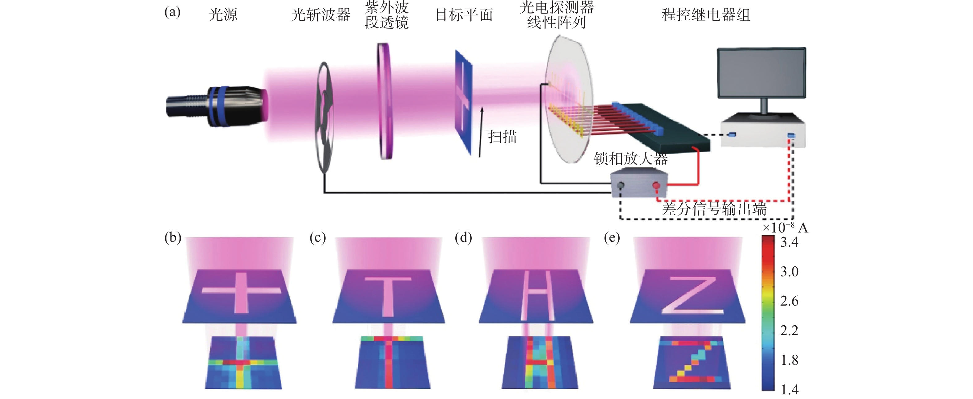
ZHANG Z F, LIN C N, YANG X, et al. Solar-blind imaging based on 2-inch polycrystalline diamond photodetector linear array [J]. Carbon,2021,173:427-432. doi: 10.1016/j.carbon.2020.11.013
|
| [96] |
ZHANG Z F, LIN C N, YANG X, et al. Wafer-sized polycrystalline diamond photodetector planar arrays for solar-blind imaging [J]. Journal of Materials Chemistry C,2022,10(16):6488-6496. doi: 10.1039/D2TC00327A
|
Figures(9) / Tables(4)
Supported by:
Beijing Renhe Information Technology Co., Ltd.


 Email Alerts
 RSS
RSS DownLoad: