Advances in studies and applications of thick diamond films prepared by microwave plasma chemical vapor deposition
-
摘要: 近年来,随着化学气相沉积(CVD)制备金刚石技术的发展,关于金刚石的研究与应用受到越来越多的关注。目前,主要的CVD技术有微波等离子体化学气相沉积(MPCVD)、热丝化学气相沉积、直流电弧等离子体喷射化学气相沉积和热阴极等离子体化学气相沉积等。MPCVD技术因其生长的金刚石品质高,被认为是制备大面积、高质量金刚石厚膜的最佳方法。首先介绍MPCVD的基本原理和设备,比较几种主要MPCVD技术的优缺点,并对国内外的研究进展进行总结,包括金刚石生长工艺的研究,特别是国内外单晶/多晶金刚石厚膜的制备研究,然后总结近年来金刚石厚膜在电子、光学、热沉等高新技术领域的应用,最后对金刚石厚膜的发展前景进行展望。
-
关键词:
- 金刚石厚膜 /
- 微波等离子体化学气相沉积(MPCVD) /
- CVD设备
Abstract:Significance With the wide range of important applications of diamond, the demand for large-area diamond has been increasing in recent years. Compared to other chemical vapor deposition (CVD) methods, the microwave plasma chemical vapor deposition (MPCVD) method is recognized as the best technology for depositing high-quality diamond films. To realize CVD diamond thick films for optical, electrical, and thermal applications, it is necessary to meet the requirements in terms of crystalline quality, optical transmittance, thermal conductivity, size, thickness, and strength. Therefore, obtaining diamond materials with sufficient size and quality is the foundation of their applications. Especially since this century, MPCVD equipment and processes have made breakthroughs, and the preparations of single crystal diamond and high-quality polycrystalline diamond thick films have been successfully realized. This paper introduces the principles and process of preparing diamond thick films by MPCVD, and summarizes the research and application progress of MPCVD-prepared diamond films at home and abroad in recent years. Our views on the future development of MPCVD-prepared diamond films are also proposed in this paper. Progress The MPCVD equipment originated overseas, initially developed by Japanese scientist Yoshihiko Kuriyama and researchers from Nippon Electric Company around the 1980s. Subsequently, countries such as Germany, Britain, the United States, and Russia also engaged in research and development efforts. The evolution of MPCVD chambers has seen a transition from quartz tubes and quartz bell jars to cylindrical resonance chambers, loop antennas, and ellipsoidal resonance chambers. Concurrently, power output has escalated from hundreds of watts to thousands and tens of kilowatts. The advancement of MPCVD technology was spearheaded by foreign entities like E6 (UK), Michigan State University (USA), and the Institute of Applied Physics (Russia), which gradually increased power levels and evolved cavity designs. With progress in diamond film deposition technology and ongoing exploration of microwave sources, higher-power 915 MHz MPCVD systems have been developed. The longer wavelength of 915 MHz microwaves enables these devices to achieve higher power levels, which facilitates an increase in the deposition rate and quality of diamond films, as well as the capability to produce larger-sized diamond films. Domestic development of MPCVD technology began relatively late, with institutions such as the University of Science and Technology Beijing, Hebei Province Laser Research Institute, and Xi'an University of Electronic Science and Technology developing 2.45 GHz and 915 MHz MPCVD equipment after the year 2000. Diamonds possess a high refractive index and significant dispersion, exhibiting superior thermal, mechanical, and optical properties. High-quality polycrystalline diamond films synthesized via the MPCVD method closely resemble natural type IIa diamonds in many aspects. Consequently, MPCVD-prepared diamond films have found extensive applications in optical window materials, thermal management, semiconductor devices, quantum technology, and optoelectronic devices. The third section of the paper provides a detailed account of the progress in applied research within these areas. Conclusions and Prospects Diamond is a material of significant interest and extensive research in the contemporary world. Over the decades, CVD diamond technology has matured, with preparation processes becoming well-established and the equipment continuously evolving and refining. Among the various CVD techniques, MPCVD equipment has seen particularly rapid development. Through persistent exploration, research, and development, the performance gap between domestically produced 2.45 GHz and 915 MHz MPCVD equipment in China and their foreign counterparts is narrowing, although there is still room for improvement in terms of power enhancement, equipment stability, and cavity design. MPCVD-method-prepared diamond thick films hold great promise for a variety of high-tech applications, including optics, thermal management, and electronics. However, their growth rate, size, and uniformity remain areas that require further attention. Looking ahead, ongoing research is essential in several key areas: optimizing and enhancing equipment, refining the growth process, and innovating process parameters (such as atmosphere, power, and substrate) to achieve higher growth rates, superior quality, and reduced costs. These efforts aim to meet the demands of commercialization, thereby facilitating the widespread adoption of diamond thick films in thermal deposition and optical applications. -
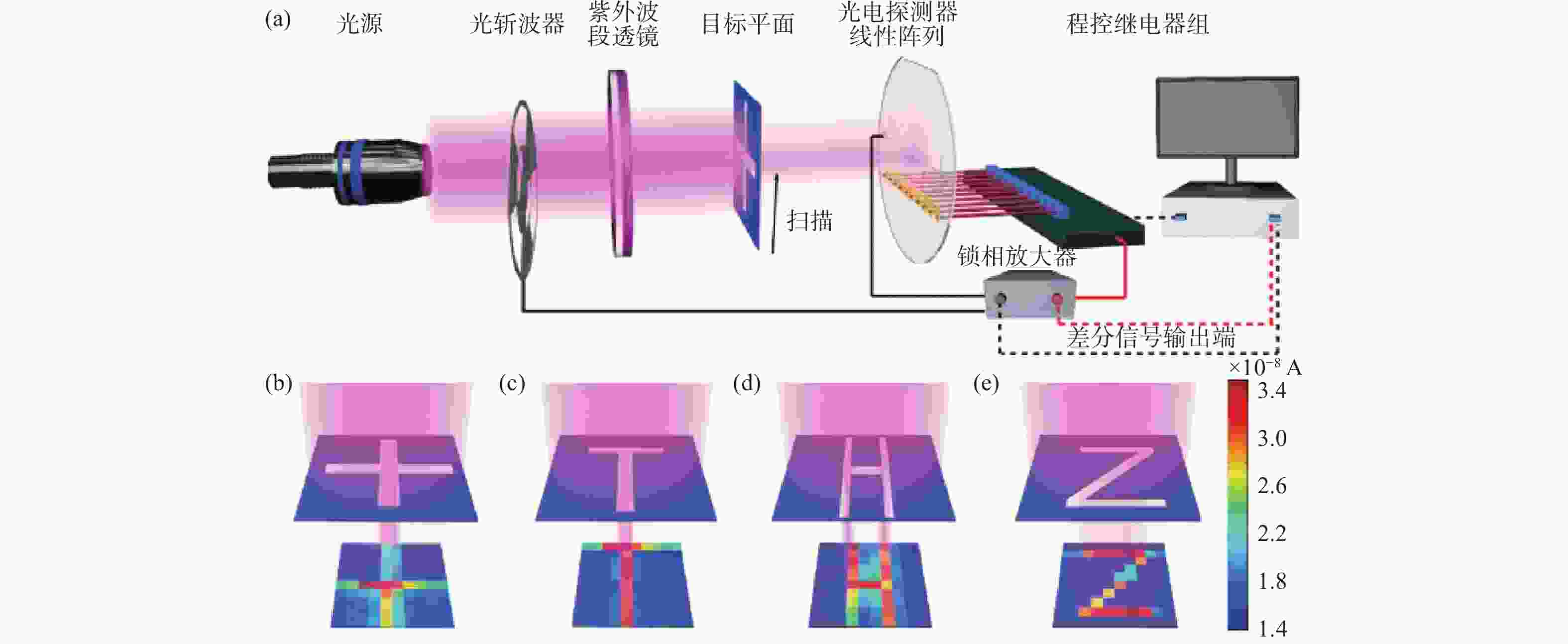
图 9 (a)基于多晶金刚石光电探测器线性阵列的成像系统示意图(b)~(e)显示从具有不同光学图案的光电探测器线性阵列获得的相应成像结果[95]
Figure 9. (a) Schematic of imaging system based on polycrystalline diamond photodetector linear array (b)~(e) Bottom figures show corresponding imaging results acquired from photodetector linear array with different optical patterns[95]
腔室类型 开始时间 最初研究单位 微波功率 P / kW 缺点 石英管式 20世纪80年代初 日本无机材料研究所 膜质量低、速率慢,石英管污染导致微波功率受限 石英钟罩式 20世纪80年代末 德国philips、美国ASTeX(现Seki) 1~3 石英钟罩污染导致微波功率受限 圆柱谐振腔式 1992年前后 美国ASTeX(现Seki) 1~5 石英窗易受等离子影响而损毁 环形天线式 1993年 美国ASTeX(现Seki) 6~8 沉积条件、谐振状态无法调整和优化 椭球谐振腔式 1997年前后 德国Fraunhofer研究所 6  下载: 导出CSV
腔室类型 研究单位 微波功率 P / kW 沉积速率 V / (μm·h−1) 沉积直径 D 石英管式 日本近畿大学 1和7 1和50 10 mm 石英钟罩式 美国密歇根州立大学 30 0.03~0.46 10~20 cm 环形天线式 美国ASTeX(现Seki) 60~100 10 8 in 椭球谐振腔式 德国Fraunhofer研究所 60 1~15 150 mm
下载: 导出CSV
表 3 沉积气体对MPCVD金刚石膜的影响
Table 3. Effect of deposition gas on MPCVD diamond film
气体 对沉积速率的影响 主要作用 CH4 提高 随着CH4浓度的增加,碳氢基团比例增加,沉积速率增加,但过量的CH4会形成非金刚石石墨相,使质量下降 H2 降低 刻蚀生长过程中产生的非金刚石相,对金刚石也有微弱的刻蚀作用 CO2 提高 刻蚀非金刚石相,促进CH4解离,提升金刚石质量 O2 提高 提高金刚石纯度,过量O2不利于金刚石生长 N2 提高 较大程度地提升金刚石沉积速率和质量,但会引入氮缺陷 Ar 提高 提高金刚石生长的均匀性
下载: 导出CSV
-
[1] 林晓棋, 满卫东, 张玮, 等. MPCVD法合成大单晶金刚石的研究进展 [J]. 硬质合金,2013,30(5):288-296.LIN Xiaoqi, MAN Weidong, ZHANG Wei, et al. Research progress on synthesis of large-scale single crystal diamond by MPCVD [J]. Cemented Carbide,2013,30(5):288-296. [2] SCHRECK M, GSELL S, BRESCIA R, et al. Ion bombardment induced buried lateral growth: The key mechanism for the synthesis of single crystal diamond wafers [J]. Scientific Reports,2017,7:44462. doi: 10.1038/srep44462 [3] 吕反修. 金刚石膜制备与应用:下卷 [M]. 北京: 科学出版社, 2014.LYU Fanxiu. Preparation and application of diamond film: Volume 2 [M]. Beijing: Science Press, 2014. [4] BUNDY F P, HALL H T, STRONG H M, et al. Man-made diamonds [J]. Nature,1955,176(4471):51-55. doi: 10.1038/176051a0 [5] ANGUS J C, WILL H A, STANKO W S. Growth of diamond seed crystals by vapor deposition [J]. Journal of Applied Physics, 1968, 39(6): 2915-2922. doi: 10.1063/1.1656693 [6] GORDON M H, DUTEN X, HASSOUNI K, et al. Energy coupling efficiency of a hydrogen microwave plasma reactor [J]. Journal of Applied Physics, 2001, 89(3): 1544-1549. doi: 10.1063/1.1337593 [7] VIKHAREV A L, GORBACHEV A M, KOZLOV A V, et al. Microcrystalline diamond growth in presence of argon in millimeter-wave plasma-assisted CVD reactor [J]. Diamond and Related Materials,2008,17(7/8/9/10):1055-1061. doi: 10.1016/j.diamond.2008.01.050 [8] YAMAMOTO M, TERAJI T, ITO T. Improvement in the crystalline quality of homoepitaxial diamond films by oxygen plasma etching of mirror-polished diamond substrates [J]. Journal of Crystal Growth,2005,285(1/2):130-136. doi: 10.1016/j.jcrysgro.2005.08.019 [9] LIN C R, LIAO W H, WEI D H, et al. Fabrication of highly transparent ultrananocrystalline diamond films from focused microwave plasma jets [J]. Surface and Coatings Technology,2013,231:594-598. doi: 10.1016/j.surfcoat.2012.01.052 [10] FENDRYCH F, TAYLOR A, PEKSA L, et al. Growth and characterization of nanodiamond layers prepared using the plasma-enhanced linear antennas microwave CVD system [J]. Journal of Physics D: Applied Physics,2010,43(37):374018. doi: 10.1088/0022-3727/43/37/374018 [11] 刘金龙, 安康, 陈良贤, 等. CVD金刚石自支撑膜的研究进展 [J]. 表面技术,2018,47(4):1-10. doi: 10.16490/j.cnki.issn.1001-3660.2018.04.001LIU Jinlong, AN Kang, CHEN Liangxian, et al. Research progress of free-standing CVD diamond films [J]. Surface Technology,2018,47(4):1-10. doi: 10.16490/j.cnki.issn.1001-3660.2018.04.001 [12] ASKARI S J, CHEN G C, LU F X. Growth of polycrystalline and nanocrystalline diamond films on pure titanium by microwave plasma assisted CVD process [J]. Materials Research Bulletin,2008,43(5):1086-1092. doi: 10.1016/j.materresbull.2007.06.010 [13] SU J J, LI Y F, LI X L, et al. A novel microwave plasma reactor with a unique structure for chemical vapor deposition of diamond films [J]. Diamond and Related Materials,2014,42:28-32. doi: 10.1016/j.diamond.2013.12.001 [14] 李义锋. 新型高功率MPCVD装置研制与金刚石膜高效沉积 [D]. 北京: 北京科技大学, 2015.LI Yifeng. Development of a new high power MPCVD device and efficient deposition of diamond films [D]. Beijing: University of Science and Technology Beijing, 2015. [15] 李义锋, 唐伟忠, 姜龙, 等. 915MHz高功率MPCVD装置制备大面积高品质金刚石膜 [J]. 人工晶体学报,2019,48(7):1262-1267. doi: 10.3969/j.issn.1000-985X.2019.07.013LI Yifeng, TANG Weizhong, JIANG Long, et al. Large area high quality diamond films deposition by 915 MHz high power MPCVD reactor [J]. Journal of Synthetic Crystals,2019,48(7):1262-1267. doi: 10.3969/j.issn.1000-985X.2019.07.013 [16] 佚名. 微波等离子体化学气相沉积系统简介及研发进展[EB/OL]. (2020-07-10)[2023-07-13]. http://www.xdwh-inst.com/display/349355.html.Anonymous. Introduction and development progress of microwave plasma chemical vapor deposition system[EB/OL]. (2020-07-10)[2023-07-13]. http://www.xdwh-inst.com/display/349355.html. [17] SHIH H C, SUNG C P, TANG Y S, et al. Microstructure and characterization of diamond film grown on various substrates [J]. Surface and Coatings Technology,1992,52(2):105-114. doi: 10.1016/0257-8972(92)90034-8 [18] SEDOV V, MARTYANOV A, ALTAKHOV A, et al. Effect of substrate holder design on stress and uniformity of large-area polycrystalline diamond films grown by microwave plasma-assisted CVD [J]. Coatings,2020,10(10):939. doi: 10.3390/coatings10100939 [19] BOLSHAKOV A P, RALCHENKO V G, YUROV V Y, et al. Enhanced deposition rate of polycrystalline CVD diamond at high microwave power densities [J]. Diamond and Related Materials,2019,97:107466. doi: 10.1016/j.diamond.2019.107466 [20] MITSUDA Y, KOJIMA Y, YOSHIDA T, et al. The growth of diamond in microwave plasma under low pressure [J]. Journal of Materials Science,1987,22(5):1557-1562. doi: 10.1007/BF01132374 [21] 张青, 翁俊, 刘繁, 等. 高功率微波等离子体对单晶金刚石同质外延生长的影响 [J]. 表面技术,2022,51(6):364-373,398. doi: 10.16490/j.cnki.issn.1001-3660.2022.06.035ZHANG Qing, WENG Jun, LIU Fan, et al. Effect of high microwave power plasma on the homogeneous epitaxy growth of single crystal diamond [J]. Surface Technology,2022,51(6):364-373,398. doi: 10.16490/j.cnki.issn.1001-3660.2022.06.035 [22] MANDAL S. Nucleation of diamond films on heterogeneous substrates: A review [J]. RSC Advances,2021,11(17):10159-10182. doi: 10.1039/D1RA00397F [23] TANG C J, FERNANDES A J S, JIANG X F, et al. Effect of methane concentration in hydrogen plasma on hydrogen impurity incorporation in thick large-grained polycrystalline diamond films [J]. Journal of Crystal Growth,2015,426:221-227. doi: 10.1016/j.jcrysgro.2015.06.018 [24] 罗凯, 汪建华, 余军火, 等. 高功率微波等离子体环境下甲烷浓度对金刚石膜的影响 [J]. 化工学报,2018,69(S2):505-511. doi: 10.11949/j.issn.0438-1157.20181169LUO Kai, WANG Jianhua, YU Junhuo, et al. Effect of methane concentration on diamond film in high power microwave plasma environment [J]. CIESC Journal,2018,69(S2):505-511. doi: 10.11949/j.issn.0438-1157.20181169 [25] MÜLLER-SEBERT W, WÖRNER E, FUCHS F, et al. Nitrogen induced increase of growth rate in chemical vapor deposition of diamond [J]. Applied Physics Letters,1996,68(6):759-760. doi: 10.1063/1.116733 [26] SEDOV V, MARTYANOV A, SAVIN S, et al. CVD synthesis of multi-layered polycrystalline diamond films with reduced roughness using time-limited injections of N2 gas [J]. Diamond and Related Materials,2021,114:108333. doi: 10.1016/j.diamond.2021.108333 [27] 王蒙, 翁俊, 刘繁, 等. 氩气对高功率MPCVD制备金刚石膜的影响 [J]. 化学工程与装备,2021(10):5-6. doi: 10.19566/j.cnki.cn35-1285/tq.2021.10.003WANG Meng, WENG Jun, LIU Fan, et al. Effect of argon on diamond films prepared by high power MPCVD [J]. Chemical Engineering & Equipment,2021(10):5-6. doi: 10.19566/j.cnki.cn35-1285/tq.2021.10.003 [28] CHEIN T H, WEI J, TZENG Y. Synthesis of diamond in high power-density microwave methane/hydrogen/oxygen plasmas at elevated substrate temperatures [J]. Diamond and Related Materials,1999,8(8/9):1686-1696. doi: 10.1016/S0925-9635(99)00059-X [29] ANDO Y, YOKOTA Y, TACHIBANA T, et al. Large area deposition of 〈100〉-textured diamond films by a 60-kW microwave plasma CVD reactor [J]. Diamond and Related Materials,2002,11(3/4/5/6):596-600. doi: 10.1016/S0925-9635(02)00018-3 [30] HEMAWAN K W, GROTJOHN T A, REINHARD D K, et al. Improved microwave plasma cavity reactor for diamond synthesis at high-pressure and high power density [J]. Diamond and Related Materials,2010,19(12):1446-1452. doi: 10.1016/j.diamond.2010.07.005 [31] KAMO M, SATO Y, MATSUMOTO S, et al. Diamond synthesis from gas phase in microwave plasma [J]. Journal of Crystal Growth,1983,62(3):642-644. doi: 10.1016/0022-0248(83)90411-6 [32] RALCHENKO V G, SAVELIEV A V, POPOVICH A F, et al. CVD diamond coating of AlN ceramic substrates to enhance heat removal [J]. Russian Microelectronics,2006,35(4):205-209. doi: 10.1134/S1063739706040019 [33] VIKHAREV A L, GORBACHEV A M, LOBAEV M A, et al. Multimode cavity type MPACVD reactor for large area diamond film deposition [J]. Diamond and Related Materials,2018,83:8-14. doi: 10.1016/j.diamond.2018.01.011 [34] HONG S P, LEE K I, YOU H J, et al. Scanning deposition method for large-area diamond film synthesis using multiple microwave plasma sources [J]. Nanomaterials,2022,12(12):1959. doi: 10.3390/nano12121959 [35] RIFAI A, CREEDON D, TRAN N, et al. Highly uniform polycrystalline diamond coatings of three-dimensional structures [J]. Surface and Coatings Technology,2021,408:126815. doi: 10.1016/j.surfcoat.2020.126815 [36] FÜNER M, WILD C, KOIDL P. Simulation and development of optimized microwave plasma reactors for diamond deposition [J]. Surface and Coatings Technology,1999,116:853-862. doi: 10.1016/S0257-8972(99)00233-9 [37] YAMADA H, CHAYAHARA A, UMEZAWA H, et al. Fabrication and fundamental characterizations of tiled clones of single-crystal diamond with 1-inch size [J]. Diamond and Related Materials,2012,24:29-33. doi: 10.1016/j.diamond.2011.09.007 [38] YAMADA H, CHAYAHARA A, MOKUNO Y, et al. Uniform growth and repeatable fabrication of inch-sized wafers of a single-crystal diamond [J]. Diamond and Related Materials,2013,33:27-31. doi: 10.1016/j.diamond.2012.12.012 [39] YAMADA H, CHAYAHARA A, MOKUNO Y, et al. A 2-in. mosaic wafer made of a single-crystal diamond [J]. Applied Physics Letters, 14, 104(10): 102110. [40] 佚名. 金刚石半导体越来越近[EB/OL]. (2022-04-04)[2024-04-15]. https://baijiahao.baidu.com/s?id=1762216523971146798&wfr=spider&for=pc.Anonymous. Diamond semiconductors are getting closer and closer [EB/OL]. (2022-04-04)[2024-04-15]. https://baijiahao.baidu.com/s?id=1762216523971146798&wfr=spider&for=pc. [41] DT半导体材料. 全球首个!100 mm的金刚石晶圆面世 [EB/OL]. (2023-1-08)[2024-04-16]. https://www.eet-china.com/mp/a264952.htmlDT semiconductor material. World’s first diamond wafer [EB/OL]. (2023-1-08)[2024-04-16]. https://www.eet-china.com/mp/a264952.html. [42] SU J J, LI Y F, DING M H, et al. A dome-shaped cavity type microwave plasma chemical vapor deposition reactor for diamond films deposition [J]. Vacuum,2014,107:51-55. [43] LI X J, TANG W Z, YU S W, et al. Design of novel plasma reactor for diamond film deposition [J]. Diamond and Related Materials,2011,20(4):480-484. doi: 10.1016/j.diamond.2011.01.046 [44] LI Y F, SU J J, LIU Y Q, et al. Design of a new TM021 mode cavity type MPCVD reactor for diamond film deposition [J]. Diamond and Related Materials,2014,44:88-94. doi: 10.1016/j.diamond.2014.02.010 [45] LI Y F, AN X M, LIU X C, et al. A 915MHz/75kW cylindrical cavity type microwave plasma chemical vapor deposition reactor with a ladder-shaped circumferential antenna developed for growing large area diamond films [J]. Diamond and Related Materials,2017,78:67-72. doi: 10.1016/j.diamond.2017.08.007 [46] 张帅, 安康, 杨志亮, 等. 新型MPCVD沉积模式制备高均匀性的D100 mm金刚石薄膜 [J]. 真空与低温,2022,28(5):549-555. doi: 10.3969/j.issn.1006-7086.2022.05.008ZHANG Shuai, AN Kang, YANG Zhiliang, et al. 100 mm in diameter diamond films with high uniformity prepared by novel deposition mode in MPCVD system [J]. Vacuum and Cryogenics,2022,28(5):549-555. doi: 10.3969/j.issn.1006-7086.2022.05.008 [47] 于盛旺, 安康, 李晓静, 等. 高功率MPCVD金刚石膜红外光学材料制备 [J]. 红外与激光工程,2013,42(4):971-974. doi: 10.3969/j.issn.1007-2276.2013.04.025YU Shengwang, AN Kang, LI Xiaojing, et al. Preparation of diamond films as an infrared optical material by high power microwave plasma CVD [J]. Infrared and Laser Engineering,2013,42(4):971-974. doi: 10.3969/j.issn.1007-2276.2013.04.025 [48] 于盛旺, 刘艳青, 唐伟忠, 等. 高功率MPCVD金刚石膜透波窗口材料制备研究 [J]. 人工晶体学报,2012,41(4):896-899. doi: 10.3969/j.issn.1000-985X.2012.04.014YU Shengwang, LIU Yanqing, TANG Weizhong, et al. Synthesis of diamond film as electromagnetic window material by an ellipsoidal MPCVD reactor at high input microwave power levels [J]. Journal of Synthetic Crystals,2012,41(4):896-899. doi: 10.3969/j.issn.1000-985X.2012.04.014 [49] YU S W, WANG R, ZHENG K, et al. Influence of power density on high purity 63 mm diameter polycrystalline diamond deposition inside a 2.45 GHz MPCVD reactor [J]. Journal of Physics D: Applied Physics,2016,49(35):355202. doi: 10.1088/0022-3727/49/35/355202 [50] LI X J, ZHOU S, CHEN G, et al. Systematic research on the performance of self-designed microwave plasma reactor for CVD high quality diamond [J]. Defence Technology,2018,14(5):373-379. doi: 10.1016/j.dt.2018.05.004 [51] 杨国永, 熊绍阳, 鲁云祥, 等. 大尺寸自支撑金刚石膜制备工艺及其红外透过性能研究 [J]. 硬质合金,2020,37(5):350-356. doi: 10.3969/j.issn.1003-7292.2020.05.004YANG Guoyong, XIONG Shaoyang, LU Yunxiang, et al. Study of large-area free-standing diamond films and its property of infrared transmittance [J]. Cemented Carbide,2020,37(5):350-356. doi: 10.3969/j.issn.1003-7292.2020.05.004 [52] 佚名. 郑州大学研制出两英寸光学级金刚石晶体[EB/OL]. (2019-09-26)[2023-07-14]. https://www.nsfc.gov.cn/csc/20340/20289/45388/index.html.Anonymous. Zhengzhou University has developed two inch optical grade diamond crystals [EB/OL]. (2019-09-26)[2023-07-14]. https://www.nsfc.gov.cn/csc/20340/20289/45388/index.html. [53] 梁天, 汪建华, 翁俊, 等. 高气压对MPCVD沉积金刚石薄膜的影响 [J]. 真空与低温,2018,24(1):54-59. doi: 10.3969/j.issn.1006-7086.2018.01.010LIANG Tian, WANG Jianhua, WENG Jun, et al. Influence of high pressure on MPCVD deposition of diamond films [J]. Vacuum and Cryogenics,2018,24(1):54-59. doi: 10.3969/j.issn.1006-7086.2018.01.010 [54] 丁康俊, 马志斌, 宋修曦, 等. 温度对MPCVD法同质外延单晶金刚石缺陷的影响 [J]. 金刚石与磨料磨具工程,2018,38(2):8-11,19. doi: 10.13394/j.cnkij.gszz.2018.2.0002DING Kangjun, MA Zhibin, SONG Xiuxi, et al. Effect of temperature on defects in homoepitaxial single crystal diamond by MPCVD [J]. Diamond & Abrasives Engineering,2018,38(2):8-11,19. doi: 10.13394/j.cnkij.gszz.2018.2.0002 [55] 夏禹豪, 李艳春, 耿传文, 等. MPCVD中双基片台结构对单晶金刚石生长的影响 [J]. 金刚石与磨料磨具工程,2018,38(3):1-5. doi: 10.13394/j.cnki.jgszz.2018.3.0001XIA Yuhao, LI Yanchun, GENG Chuanwen, et al. Influence of dual-substrate structure on growth of single crystal diamond by MPCVD [J]. Diamond & Abrasives Engineering,2018,38(3):1-5. doi: 10.13394/j.cnki.jgszz.2018.3.0001 [56] 夏禹豪, 耿传文, 衡凡, 等. MPCVD法中氮气对单晶金刚石生长机理影响的探究 [J]. 真空科学与技术学报,2018,38(8):684-688. doi: 10.13922/j.cnki.cjovst.2018.08.07XIA Yuhao, GENG Chuanwen, HENG Fan, et al. Impact of nitrogen concentration on monocrystalline diamond growth in microwave plasma chemical vapor deposition [J]. Chinese Journal of Vacuum Science and Technology,2018,38(8):684-688. doi: 10.13922/j.cnki.cjovst.2018.08.07 [57] 王斌, 汪建华, 翁俊, 等. 气体流动方式对MPCVD金刚石薄膜均匀性的影响 [J]. 真空与低温,2020,26(2):108-113. doi: 10.3969/j.issn.1006-7086.2020.02.004WANG Bin, WANG Jianhua, WENG Jun, et al. Effect of gas flow mode on uniformity of MPCVD diamond films [J]. Vacuum and Cryogenics,2020,26(2):108-113. doi: 10.3969/j.issn.1006-7086.2020.02.004 [58] 何中文, 马志斌. 高等离子体功率密度下MPCVD法制备多晶金刚石膜 [J]. 金刚石与磨料磨具工程,2022,42(2):156-161. doi: 10.13394/J.cnki.jgszz.2021.0121HE Zhongwen, MA Zhibin. Preparation of polycrystalline diamond films by MPCVD at high plasma power density [J]. Diamond & Abrasives Engineering,2022,42(2):156-161. doi: 10.13394/J.cnki.jgszz.2021.0121 [59] WANG Q J, WU G, LIU S, et al. Simulation-based development of a new cylindrical-cavity microwave-plasma reactor for diamond-film synthesis [J]. Crystals,2019,9(6):320. doi: 10.3390/cryst9060320 [60] YANG B, SHEN Q, GAN Z Y, et al. Analysis of improving the edge quality and growth rate of single-crystal diamond growth using a substrate holder [J]. CrystEngComm,2019,21(43):6574-6584. doi: 10.1039/C9CE01402K [61] BANERJEE A, BERNOULLI D, ZHANG H T, et al. Ultralarge elastic de-formation of nanoscale diamond [J]. Science,2018,360(6386):300-302. doi: 10.1126/science.aar4165 [62] 陈良贤, 刘金龙, 冯寅楠, 等. 金刚石上不同晶体结构Y2O3膜性质与增透性能研究 [J]. 表面技术,2019,48(1):133-140. doi: 10.16490/j.cnki.issn.1001-3660.2019.01.017CHEN Liangxian, LIU Jinlong, FENG Yinnan, et al. Properties and anti-reflection performance of Y2O3 films with different crystal structures on diamond [J]. Surface Technology,2019,48(1):133-140. doi: 10.16490/j.cnki.issn.1001-3660.2019.01.017 [63] 左杨平, 卢文壮, 张圣斌, 等. 面向激光防护应用的金刚石/V2O5膜系设计与制备 [J]. 红外与激光工程,2015,44(8):2491-2495. doi: 10.3969/j.issn.1007-2276.2015.08.042ZUO Yangping, LU Wenzhuang, ZHANG Shengbin, et al. Design and fabrication of diamond/V2O5 films in continuous laser protection [J]. Infrared and Laser Engineering,2015,44(8):2491-2495. doi: 10.3969/j.issn.1007-2276.2015.08.042 [64] 吕反修, 高旭辉, 郭会斌, 等. 在预涂陶瓷过渡层的多谱段ZnS衬底上沉积金刚石膜的探索研究 [J]. 人工晶体学报,2004,33(1):105-108. doi: 10.3969/j.issn.1000-985X.2004.01.023LYU Fanxiu, GAO Xuhui, GUO Huibin, et al. An exploratory study on preparation of diamond film coatings on multi-spectra ZnS pre-coated with a ceramic interlayer [J]. Journal of Synthetic Crystals,2004,33(1):105-108. doi: 10.3969/j.issn.1000-985X.2004.01.023 [65] 黄亚博, 陈良贤, 贾鑫, 等. CVD金刚石表面增透膜的研究进展 [J]. 表面技术,2020,49(10):106-117. doi: 10.16490/j.cnki.issn.1001-3660.2020.10.012HUANG Yabo, CHEN Liangxian, JIA Xin, et al. Research progress of anti-reflection films on CVD diamond surface [J]. Surface Technology,2020,49(10):106-117. doi: 10.16490/j.cnki.issn.1001-3660.2020.10.012 [66] 白振旭, 杨学宗, 陈晖, 等. 高功率金刚石激光技术研究进展(特邀) [J]. 红外与激光工程,2020,49(12):9-21. doi: 10.3788/IRLA20201076BAI Zhenxu, YANG Xuezong, CHEN Hui, et al. Research progress of high-power diamond laser technology(Invited) [J]. Infrared and Laser Engineering,2020,49(12):9-21. doi: 10.3788/IRLA20201076 [67] 王伟华, 代兵, 王杨, 等. 金刚石光学窗口相关元件的研究进展 [J]. 材料科学与工艺,2020,28(3):42-57. doi: 10.11951/j.issn.1005-0299.20200074WANG Weihua, DAI Bing, WANG Yang, et al. Recent progress of diamond optical window-related components [J]. Materials Science and Technology,2020,28(3):42-57. doi: 10.11951/j.issn.1005-0299.20200074 [68] Optics: Enable extreme performance photonics [EB/OL]. [2021-07-14]. https://www.e6.com/en/knowledge-base/brochures. [69] 李凤凤, 刘永佳, 张建华. 培育钻石的发展现状及应用研究 [J]. 超硬材料工程,2022,34(4):51-54. doi: 10.3969/j.issn.1673-1433.2022.04.011LI Fengfeng, LIU Yongjia, ZHANG Jianhua. Development status and application of diamond cultivation [J]. Superhard Material Engineering,2022,34(4):51-54. doi: 10.3969/j.issn.1673-1433.2022.04.011 [70] 王光祖, 位星, 张相法, 等. 饰钻培育技术的由来与兴起 [J]. 超硬材料工程,2022,34(5):42-47. doi: 10.3969/j.issn.1673-1433.2022.05.010WANG Guangzu, WEI Xing, ZHANG Xiangfa, et al. Origin and rise of decorative diamond cultivation technology [J]. Superhard Material Engineering,2022,34(5):42-47. doi: 10.3969/j.issn.1673-1433.2022.05.010 [71] 佚名. GIA鉴定34.59克拉化学气相沉积法(CVD)实验室培育钻石 [EB/OL]. (2023-05-29)[2023-07-14]. https://baijiahao.baidu.com/s?id=1767205622858628324&wfr=spider&for=pc.Anonymous. GIA Identification 34.59 Carat Chemical Vapor Deposition (CVD) Laboratory Cultivated Diamond [EB/OL]. (2023-05-29)[2023-07-14]. https://baijiahao.baidu.com/s?id=1767205622858628324&wfr=spider&for=pc. [72] CVD diamond: The element six diamond handbook [EB/OL]. [2021-07-14]. https://www.e6.com/zh/products/optics. [73] 杨士奇, 任泽阳, 张金风, 等. 硅基氮化镓异质结材料与多晶金刚石集成生长研究 [J]. 固体电子学研究与进展,2021,41(1):18-23. doi: 10.19623/j.cnki.rpsse.2021.01.005YANG Shiqi, REN Zeyang, ZHANG Jinfeng, et al. Research on growth of poly-crystalline diamond on Si-based GaN heterojunction material [J]. Research & Progress of SSE,2021,41(1):18-23. doi: 10.19623/j.cnki.rpsse.2021.01.005 [74] ZHOU Y, ANAYA J, POMEROY J, et al. Barrier-layer optimization for enhanced GaN-on-diamond device cooling [J]. ACS Applied Materials & Interfaces,2017,9(39):34416-34422. doi: 10.1021/acsami.7b08961 [75] WANG K, RUAN K, HU W B, et al. Room temperature bonding of GaN on diamond wafers by using Mo/Au nano-layer for high-power semiconductor devices [J]. Scripta Materialia,2020,174:87-90. doi: 10.1016/j.scriptamat.2019.08.029 [76] ZHAO Y, LI C M, LIU J L, et al. The interface and mechanical properties of a CVD single crystal diamond produced by multilayered nitrogen doping epitaxial growth [J]. Materials,2019,12(15):2492. doi: 10.3390/ma12152492 [77] LU M C. Development of diamond device-level heat spreader for the advancement of GaN HEMT power and RF electronics [J]. IEEE Transactions on Device and Materials Reliability,2023,23(4):468-485. doi: 10.1109/TDMR.2023.3310510 [78] FRANCIS D, FAILI F, BABIĆ D, et al. Formation and characterization of 4-inch GaN-on-diamond substrates [J]. Diamond and Related Materials,2010,19(2/3):229-233. [79] DELMAS W, JARZEMBSKI A, BAHR M, et al. Thermal transport and mechanical stress mapping of a compression bonded GaN/diamond interface for vertical power devices [J]. ACS Applied Materials & Interfaces,2024,16(8):11003-11012. [80] CHENG Z, MU F W, YATES L, et al. Interfacial thermal conductance across room-temperature-bonded GaN/diamond interfaces for GaN-on-diamond devices [J]. ACS Applied Materials & Interfaces,2020,12(7):8376-8384. doi: 10.1021/acsami.9b16959 [81] HU X F, GE L, LIU Z H, et al. Diamond-SiC composite substrates: A novel strategy as efficient heat sinks for GaN-based devices [J]. Carbon,2024,218:118755. doi: 10.1016/j.carbon.2023.118755 [82] 刘金龙, 朱肖华, 郭彦召, 等. 金刚石探测器材料研制与中子探测性能研究 [J]. 真空电子技术,2021(5):46-53,72. doi: 10.16540/j.cnki.cn11-2485/tn.2021.05.06LIU Jinlong, ZHU Xiaohua, GUO Yanzhao, et al. Material development and neutron detection performance of diamond detector [J]. Vacuum Electronics,2021(5):46-53,72. doi: 10.16540/j.cnki.cn11-2485/tn.2021.05.06 [83] GUO Y Z, LIU J L, LIU J W, et al. Comparison of α particle detectors based on single-crystal diamond films grown in two types of gas atmospheres by microwave plasma-assisted chemical vapor deposition [J]. International Journal of Minerals, Metallurgy and Materials,2020,27(5):703-712. doi: 10.1007/s12613-019-1944-0 [84] 李成明, 任飞桐, 邵思武, 等. 化学气相沉积(CVD)金刚石研究现状和发展趋势 [J]. 人工晶体学报,2022,51(5):759-780. doi: 10.3969/j.issn.1000-985X.2022.05.003LI Chengming, REN Feitong, SHAO Siwu, et al. Progress of chemical vapor deposition (CVD) diamond [J]. Journal of Synthetic Crystals,2022,51(5):759-780. doi: 10.3969/j.issn.1000-985X.2022.05.003 [85] TARELKIN S, BORMASHOV V, BUGA S, et al. Power diamond vertical Schottky barrier diode with 10 A forward current [J]. Physica Status Solidi (A),2015,212(11):2621-2627. doi: 10.1002/pssa.201532213 [86] LIU B J, ZHANG S, RALCHENKO V, et al. High temperature operation of logic AND gate based on diamond Schottky diodes fabricated by selective growth method [J]. Carbon,2022,197:292-300. doi: 10.1016/j.carbon.2022.06.040 [87] ARAUJO D, SUZUKI M, LLORET F, et al. Diamond for electronics: Materials, processing and devices [J]. Materials,2021,14(22):7081. doi: 10.3390/ma14227081 [88] PHAM T T. 200 V, 4 MV/cm lateral diamond [C]// 2017 IEEE International Electron Devices Meeting (IEDM), 2017. [89] LIU K, ZHANG S, LIU B J, et al. Investigating the energetic band diagrams of oxygen-terminated CVD grown E6 electronic grade diamond [J]. Carbon,2020,169:440-445. doi: 10.1016/j.carbon.2020.07.079 [90] KAWARADA H. Hydrogen-terminated diamond surfaces and interfaces [J]. Surface Science Reports,1996,26(7):205-259. doi: 10.1016/S0167-5729(97)80002-7 [91] ZHANG Q, GUO Y H, JI W T, et al. High-fidelity single-shot readout of single electron spin in diamond with spin-to-charge conversion [J]. Nature Communications,2021,12(1):1529. doi: 10.1038/s41467-021-21781-5 [92] BUCHER D B, AUDE CRAIK D P L, BACKLUND M P, et al. Quantum diamond spectrometer for nanoscale NMR and ESR spectroscopy [J]. Nature Protocols,2019,14(9):2707-2747. doi: 10.1038/s41596-019-0201-3 [93] 环球网. 全球首款金刚石量子计算教学机发布 [J]. 超硬材料工程, 2019, 31(4): 59.World Wide Web. The world's first diamond quantum computing teaching machine was released [J]. Superhard Material Engineering, 2019, 31(4): 59. [94] 佚名. 日本开发适用量子计算机的金刚石晶圆制造技术[EB/OL]. (2022-05-13)[2023-07-14]. https://baijiahao.baidu.com/s?id=1732674398077513655&wfr=spider&for=pc.Anonymous. Japan develops diamond wafer manufacturing technology suitable for quantum computers[EB/OL]. (2022-05-13)[2023-07-14]. https://baijiahao.baidu.com/s?id=1732674398077513655&wfr=spider&for=pc. [95] ZHANG Z F, LIN C N, YANG X, et al. Solar-blind imaging based on 2-inch polycrystalline diamond photodetector linear array [J]. Carbon,2021,173:427-432. doi: 10.1016/j.carbon.2020.11.013 [96] ZHANG Z F, LIN C N, YANG X, et al. Wafer-sized polycrystalline diamond photodetector planar arrays for solar-blind imaging [J]. Journal of Materials Chemistry C,2022,10(16):6488-6496. doi: 10.1039/D2TC00327A -


 点击查看大图
图(9) / 表(4)
计量
- 文章访问数: 15
- HTML全文浏览量: 5
- PDF下载量: 2
- 被引次数: 0
 邮件订阅
邮件订阅 RSS
RSS