Fabrication method of high energy beam for solid-state nanopore
-
摘要: 固态纳米孔因具有机械性能好、稳定性强、形状易控的优点,在基因检测、蛋白质检测、能量转换、物质分离以及水净化等领域显示出巨大的潜力,并引起众多研究人员关注。其中,形状可控、高效的固态纳米孔制造技术是现实固态纳米孔应用的前提。目前,在常见的固态纳米孔制造方法中,高能束制造方法具有高效率、高精度、高可控制造的优势。本文重点概述高能电子束、聚焦离子束、激光刻蚀法和离子径迹刻蚀法等4种固态纳米孔制造方法及其基本原理,并讨论上述方法的优缺点及其大规模可控制造的可行性。Abstract: Solid-state nanopores have drawn the interest of numerous researchers due to their excellent mechanical properties, stability, and shape control, which have demonstrated tremendous potential in gene detection, protein detection, energy conversion, material separation, and water purification. And shape-controlled and efficient solid-state nanopore manufacturing technology is the prerequisite for the application of solid-state nanopore. At present, the high energy beam manufacturing method has the advantages of high efficiency, high precision and high manufacturing controllability among the conventional solid state nanopore manufacturing methods. This paper provides an overview of four solid state nanopore fabrication methods including high energy electron beam, focused ion beam, laser etching and ion track etching and their fundamental principles. The benefits and drawbacks of these methods, as well as their feasibility for large-scale controlled fabrication are discussed.
-
Key words:
- solid nanopore /
- high-energy beam manufacturing /
- manufacturing method.
-
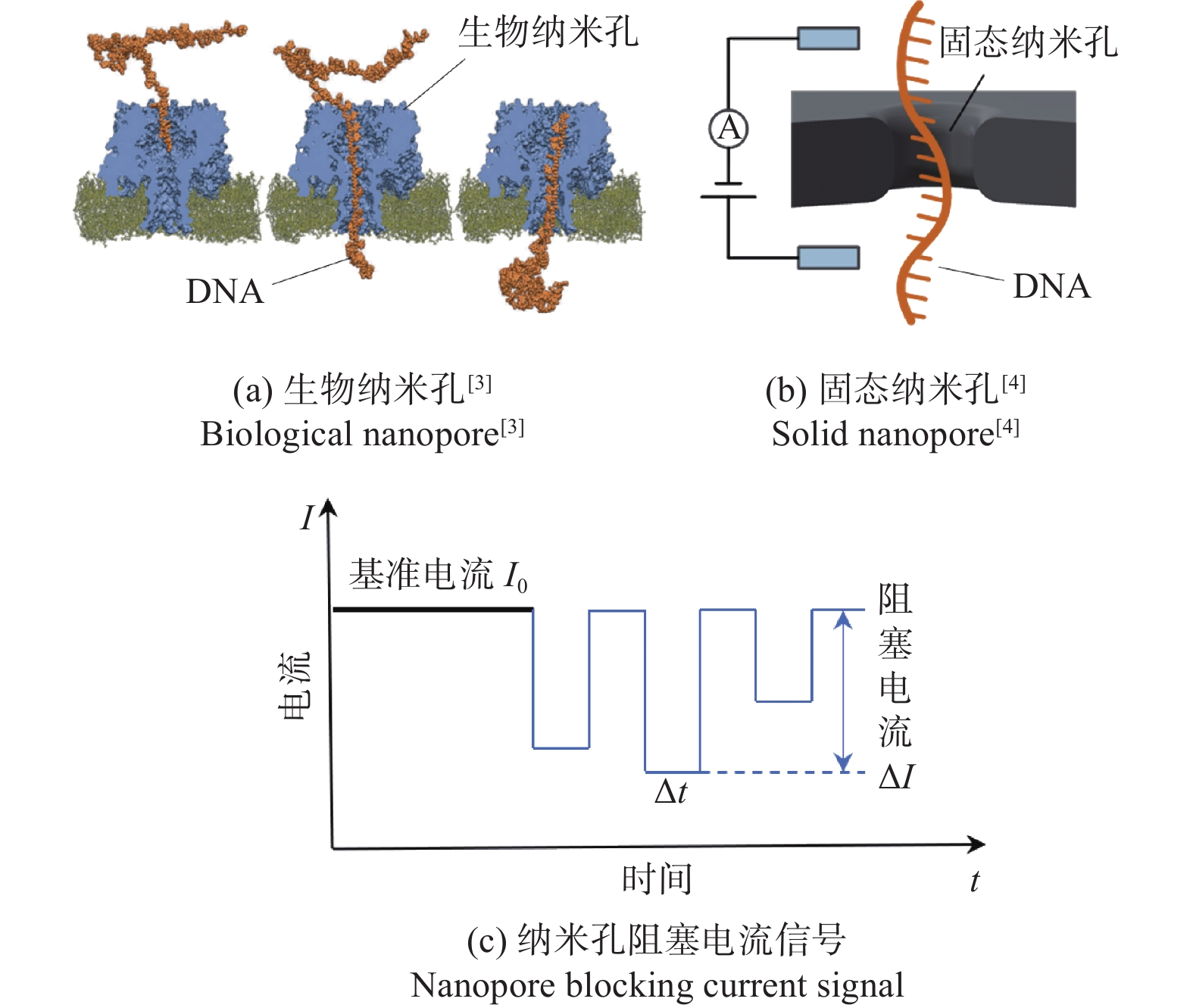
纳米孔传感器是近年来发展迅速的单分子级检测生物传感器。该传感器的工作原理如图1所示:利用纳米孔薄膜隔绝两侧溶液,在纳米孔薄膜两侧施加一定的电压,驱动带电生物分子穿过纳米孔,并引起物理占位,进而反映在离子电流中,即形成阻塞电流[1];通过分析阻塞电流信号间接获得所测生物分子信息。KASIANOWIZ等[1]在COULTER专利[2]的基础上提出了纳米孔检测方法,首次使用直径仅为2.6 nm的α-溶血素生物孔,在电场的作用下让单链DNA分子穿过纳米通道获得阻塞电流信号。通过检测阻塞电流的幅值与时间特性,原则上可以直接、快速实现单分子序列的检测。这项研究展示了纳米孔检测技术在DNA测序等单分子检测上的巨大潜力,纳米孔传感器也随之成为研究的热点之一。
目前,用于单分子传感检测的纳米孔可根据材料分为固态纳米孔和生物纳米孔。生物纳米孔主要有
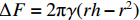
$ \alpha $ -HL[5]、MspA[6]、FraC[7]和Phi29[8]等。生物纳米孔是一种天然的蛋白质离子通道,具有重复性好、成本低、易修饰的特点。自1996年开启了生物纳米孔检测新篇章后,AKESON等[9]利用实验验证了通过$ \alpha $ -HL的离子电流信号来区别核苷酸类型的思路。之后,出现了噬菌体Phi29连接器[10]、MspA蛋白[6, 8]等通过控制DNA易位速度进而实现基因测序的方法,丰富了生物纳米孔分析技术的研究。除实验室研究外,Oxford Nanopore Technologies公司已经基于生物纳米孔研发出商用DNA测序仪平台MinION,实现了生物孔测序技术的商业化[11]。除生物纳米孔外,固态纳米孔具有稳定性强、机械性能好、形状易控等优点,且固态纳米孔尺寸可调空间大、材料种类多。这些卓越的特性显著地拓宽了固态纳米孔的多功能性和适用性,固态纳米孔制造及其应用也因此得到快速发展。目前,常见的固态纳米孔材料有氮化硅(Si3N4)[4, 12-13]、二氧化硅(SiO2)[13-14]、氧化铝(Al2O3)[15]、石墨烯(Graphene)[16]、氧化铪(HfO2)[17-18]、二硫化钼(MoS2)[19]、过渡金属硫化物(Transition metal sulfide)[20]以及聚合物薄膜[21]等,如图2所示。LI等[4]首次使用氩离子制造出直径仅为1.8 nm的氮化硅纳米孔,并利用该纳米孔对双链DNA分子进行了过孔检测分析;STORM等[13]用透射电镜高能电子束实现直径为2 nm的氧化硅纳米孔,并提出了基于高能电子束纳米孔最小表面能原理得到纳米孔直径调整原则。由于该方法集合了TEM高分辨成像反馈,实现了制造过程与表征同步,开创了固态纳米孔制造的新方法,因此引起了极大关注。DENG等[22]利用氦离子系统实现了直径为5 nm以下石墨烯纳米孔制造。氦离子技术的问世,克服了传统聚焦离子束(focused ion beam,FIB)无法制作直径小于10 nm纳米孔的难题。随后,XIA等[23]利用氦离子显微镜(helium ion microscope,HIM)实现了Si3N4纳米孔的高重现性和大面积的快速制造。
目前,固态纳米孔已经广泛应用于单分子检测,如基因检测[1]、蛋白质测序[24]、肿瘤标志物检测[25]、物质分离[26]、能量转换[27]等研究。上述应用也推动了固态纳米孔制造技术的发展。固态纳米孔制造方法主要有高能电子束[14, 28]、聚焦离子束[ 29]、离子径迹刻蚀法[30]、电介质击穿法[31-32]、纳米压印[33]、掩膜刻蚀法[34]、电化学沉积[35]等,其中以电子束、离子束和激光为代表的高能束制造方法在固态纳米孔及其阵列制造方法具有高效率、高精度、高可控制造优点,日后有望发展成为固态纳米孔制备方法的主流技术。因此本文详述高能电子束、聚焦离子束加工法、激光刻蚀法和离子径迹刻蚀的制造方法、原理及其优缺点。
1. 高能电子束制造方法
1.1 高能电子束缩孔技术
利用高能电子束制造技术制备的各种固态纳米孔的SEM图和TEM图如图3所示。高能电子束收缩方法源于DEKKER等提出的纳米孔表面能最小原理[13],即纳米孔相对薄膜的表面能变化量
$\Delta F=2{{{\text{π}}}} \gamma (rh-{r}^{2})$ ,其中$ \gamma $ 为液体表面张力,$ r $ 为纳米孔半径,$ h $ 为纳米孔长度。当纳米孔直径小于纳米孔薄膜厚度时,纳米孔在接受高能电子束辐照的时候会收缩;反之,纳米孔直径则会增大。STORM等[14]在DEKKER研究的基础上,原位观察氧化硅纳米孔在接受电子束辐照缩孔后的最小直径为2 nm,如图3a所示。实验结果进一步证实固态纳米孔表面能最小原理。此外,经能量色散X射线光谱仪(EDX)和电子能量损失谱(EELS)检测证实是纳米孔边缘材料(氧化硅)迁移导致纳米孔缩小,而不是纳米孔表面污染物[36-37]。纳米孔表面能最小原理在椭圆形氧化硅纳米孔、氮化硅/氧化硅复合孔等不同形态的氧化硅纳米孔中都得到验证。随后,KIM等[38]通过改变Si3N4纳米孔在TEM中的暴露时间和电子束辐照强度实现了直径为2~20 nm的纳米孔制造,并将制造精度提高到0.2 nm。尽管TEM技术可以在亚纳米分辨率下通过直接视觉反馈对纳米孔直径进行高精度调控,但TEM样品腔送样一次只能处理一个芯片,制约了固态纳米孔制造的效率。 图 3 利用高能电子束制造技术制备的各种固态纳米孔的SEM图和TEM图(a)利用高能电子束在SiO2薄膜上刻蚀初始直径约为6 nm的纳米孔(右上角插图),后经高强度TEM照射后孔径缩小至2 nm[15];(b)利用FIB制备初始直径约90 nm Si3N4孔,后经SEM辐照将孔缩小至5.3 nm[41](右上角插图);(c)利用聚焦电子束刻蚀得到纳米孔[51];(d)50 nm厚Si3N4膜上直径约7 nm纳米孔的横截面示意图,7 nm孔的俯视图(1),2 nm × 2 nm孔阵列倾斜视图(2)[52];(e)孔径为3.3 nm的Mg纳米孔[47],后在散焦电子束辐照下完全闭合(右上插图);(f)利用SEM制备出孔径小于5 nm的绝缘纳米孔[49]。Figure 3. SEM and TEM diagrams of various solid nanopores prepared by high-energy electron beam manufacturing technology(a) A nanopore with an initial diameter of about 6 nm is etched on the SiO2 film by high-energy electron beam (the illustration in the upper right corner), and then the pore size is reduced to 2 nm after high intensity TEM irradiation[15]; (b) The holes with initial diameter of about 45 nm Si3N4 were prepared by FIB, and then the hole was reduced to 5.3 nm [41] by SEM irradiation (illustration in the upper right corner); (c) Nanoholes are obtained by focused electron beam etching[51]; (d) Cross-sectional diagram of about 7 nm diameter nanopore on 50 nm thick Si3N4 film, top view of 7 nm hole (1), 2 nm× 2 nm inclined view of nanopore array (2)[52]; (e) Mg nanopore with a diameter of 3.3 nm [47] was completely closed under the irradiation of defocused electron beam (upper right illustration); (f) Insulated nanopores with aperture less than 5 nm were prepared by SEM[49].
为了提升固态纳米孔制造效率,ZHANG等[28, 39]提出利用具有较大样品腔的场发射扫描电子显微镜(SEM),使用其电子束辐照将初始直径为40~200 nm的Si3N4 和50~200 nm的SiO2 纳米孔的直径缩小到10 nm以下。这种SEM电子束辐照与TEM辐照的收缩机制不同。CHANG等[39]认为收缩机制可能是由辐射分解和随后硅原子向孔周边的运动产生的表面缺陷造成的,ZHANG等[28]则提出了焦耳热辅助辐照诱导扩散是造成孔收缩的原因。
YUAN等[40]使用SEM中的电子束辐照将初始直径约为90 nm氮化硅纳米孔缩小到5.3 nm(图3b)。利用纳米孔横截面材料元素与孔型变化分析,提出了Si3N4纳米孔收缩的烃类(碳氢化合物)沉积和Si3N4分解机理。当使用高能电子束照射Si3N4纳米孔时,纳米孔表面将沉积一层碳氢化合物,由于在大的倾斜角处产生更多二次电子[41],诱导的碳沉积在纳米孔的尖锐边缘处变得更加明显。该积碳层将在固有压缩应力下移动,以减小纳米孔的直径。同时,在电子束照射下Si3N4获得足够的能量以引发分解,N原子由于重量较轻大部分逸散到腔室中,而部分Si原子则扩散到烃层中并流入纳米孔;此外,少量N原子会与共价Si重新结合,并与碳氢化合物一起移动,从而使Si3N4纳米孔收缩。随着电子束的去除,碳氢化合物沉积和Si3N4的分解均在纳米孔区域附近停止。
与TEM的电子束收缩法相比,SEM具有腔体大的特点,可以一次载入多个样品,提高了纳米孔加工效率。此外,SEM电子束收缩法存在迁移材料的竞争[40],可以实现渐变尺寸纳米孔阵列制造。尽管电子束收缩方法已经应用于在绝缘体[14, 38]、半导体[42-43]、导体[13]薄膜上制造固态纳米孔,但是最终获得的固态纳米孔材料与本征纳米孔薄膜材料的差别,可能对应用带来影响。
1.2 高能电子束钻孔技术
高能电子束制造主要机理是动能转移引起的伴随直接原子位移的弹性散射和电子—电子碰撞引起的电离或激发的非弹性散射[44],是一种直接在悬空薄膜上制造所需尺寸的纳米孔的方法。由于其广泛的适用性、很高的分辨率以及良好的可重复性,高能电子束钻孔已逐渐成为直接制备固态纳米孔的主要技术。SHIM等[18]利用TEM在二氧化铪(HfO2)薄膜上钻取了尺寸为2 nm的纳米孔。PATTERSON等[45]使用高能电子束钻孔技术在石墨烯薄膜上制备直径约3.5 nm的纳米孔。WU等[46]利用电子束在Mg薄膜上钻取了不同形状的多边形纳米孔(3~8 nm)。RIGO等[47]利用TEM实现在10 nm厚的氮化硅薄膜上刻蚀直径小于1 nm的纳米孔。SPINNEY等[48]利用扫描电子显微镜(SEM)中的水蒸气辅助电子束,也成功制备了直径小于5 nm的绝缘纳米孔。目前,高能电子束直接钻孔技术已经成为在包括金属[46, 49]、金属氧化物[18]、Si3N4[47]及石墨烯[45, 50]等各种薄膜上制造超小尺寸纳米孔的首选技术。
2. 聚焦离子束加工法
与高能电子束制造法不同的是,聚焦离子束加工固态纳米孔的原理是通过聚焦离子束(FIB)轰击样品表面的目标原子,并将它们从其原始位置移开,从而实现在悬空薄膜表面纳米孔的加工[51]。近年来,FIB制造已经广泛用于在不同材料(绝缘材料、导电材料、半导体材料)的薄膜上制造纳米孔,常见用于固态纳米孔制造的离子束有氖离子(Ne + )、氩离子(Ar + )、稼离子(Ga + )、氦离子(He + )等[4, 39, 52-53]。以聚焦离子束制造技术制备的固态纳米孔的SEM和TEM图如图4所示。
 图 4 聚焦离子束制造技术制备的固态纳米孔的SEM和TEM图(a) Ar + 离子制备Si3N4纳米孔[13]; (b) Ga + 离子制备SiC纳米孔[57];(c)聚焦离子束制备的4 nm Si3N4纳米孔[55];(d) He + 离子制备CNM纳米孔[30];(e)He + 离子制备Si3N4阵列孔和单孔(右上角插图)[65];(f)石墨烯纳米孔[63]。Figure 4. SEM and TEM images of solid nanopores prepared by focused ion beam manufacturing technology(a) Preparation of Si3N4 nanopore by Ar + ion[13]; (b) Preparation of SiC nanopore by Ga + ion[57]; (c) 4 nm Si3N4 nanopore prepared by focused ion beam[55]; (d) CNM nanopore prepared by He + ion[30]; (e) Si3N4 array holes and single holes prepared by He + ions (illustration in the upper right corner)[65]; (f) Graphene nanopore[63].
LI等首次利用聚焦Ar + 离子束在500 nm厚的氮化硅薄膜上加工出了孔径为61 nm的纳米孔,然后通过缩孔技术将孔径缩小到了1.8 nm,如图4a所示。KUAN等[54]对室温下离子雕刻成形的纳米孔内部几何结构进行了研究,发现其是一个边缘半径为5.6 nm的典型火山结构。由于火山结构会限制纳米孔传感器的时空分辨率,因此这种结构并不理想,于是他们提出利用冷离子束雕刻方法来改善原先的结构,实现了边缘半径小至1 nm的超薄氮化硅纳米孔[54]。但FIB无法直接制造小尺寸纳米孔,因此GIERAK等[55]改进了Ga + 直写系统,利用Ga + 离子源在20 nm厚的SiC膜上加工出亚10 nm的纳米孔,如图4b所示。同时,Ga + 离子源FIB系统已用于加工Si3N4[56-57]纳米孔、石墨烯纳米孔和六方氮化硼(hBN)纳米孔[58]等。Ga + 离子源FIB系统相较于TEM能够一次同时加工多个芯片,加工效率高。
与传统的氩离子、镓离子源FIB系统相比,氦离子显微镜(HIM)具有原子大小尖端的氦离子源,可以制造直径更小、精度更高的纳米孔[59]。YANG等[53]使用HIM成功制造出直径小于4 nm的氮化硅纳米孔,并成功应用于DNA分子的检测。SAWAFTA等[60]通过HIM实现氮化硅纳米孔长度和直径的调控,证明HIM技术在尺寸控制方面的可重复性。除了氮化硅膜之外,HIM技术还可以用在其他薄膜材料和二维材料上快速制造纳米孔,如石墨烯[61]和二硫化钼[62]等。EMMRICH等[29]使用氦离子显微镜在1 nm厚的碳纳米膜上进一步将加工的纳米孔直径缩小至1.3 nm。与SEM纳米孔阵列制相似,HIM不仅能够快速、高精度制造纳米孔,还能够实现高重复性的纳米孔阵列制造。XIA等[23]利用HIM实现了Si3N4纳米孔的高重现性和大面积的快速制造,如图4e所示,证明在固态纳米孔的制造中,氦离子束提供了易于控制的孔径、出色的可重复性和大面积的快速制造工艺。基于HIM的离子束刻蚀技术具备快速制造、高重现性和加工精度高等优点,在纳米孔可控制造方面表现出独特的优势。
3. 激光刻蚀法
激光刻蚀是一种能够使用低功率(约10 mW)、高聚集激光和共聚焦显微镜制造直径为单个纳米的纳米孔技术[63]。激光加工技术是用高能量密度的激光束使工件材料表面局部升温、熔化或气化来逐层移走材料[63]。因此激光加工既可以加工导电材料也可以加工不导电材料,特别适合加工陶瓷、玻璃、金刚石、碳化硅、蓝宝石等超硬材料。作为一种低损伤的微纳加工技术,它在微纳制造领域有巨大的应用前景。
激光刻蚀加工技术最初是由日本理化研究所(RIKEN)提出的[64]。近年来,激光刻蚀已经在光敏聚合物[65-66]、半导体[67]或一些电解质薄膜[68]上实现结构尺寸约10 nm的纳米结构。GILBOA等[63]用约45 mW强度蓝色(波长为488 nm)激光器刻蚀独立的氮化硅膜,通过逐渐减薄薄膜直到形成纳米孔,制造出孔径为6.5 nm的单个氮化硅纳米孔。WU等[69]使用激光烧蚀和电流反馈控制方法应用于热塑性材料制造纳米孔,利用低强度激光束制造出直径小于10 nm的孔。LU等[70]用紧密聚焦的贝塞尔光束加工二氧化硅表面,通过精确控制二氧化硅的内部和表面的相互作用获得了直径约为20 nm的纳米孔。图5所示为以激光刻蚀技术制备的固态纳米孔的SEM和TEM图。
 图 5 激光刻蚀技术制备的固态纳米孔的SEM和TEM图Figure 5. SEM and TEM images of solid-state nanoholes prepared by laser etching technology
激光刻蚀也可以用于创建高密度的纳米孔阵列。GILBOA等[71]利用超快激光在特定位置刻蚀出纳米孔阵列,如图5d所示。与其他高能束刻蚀相比,激光刻蚀技术在光路设置和尺寸控制精度上还有待提高。
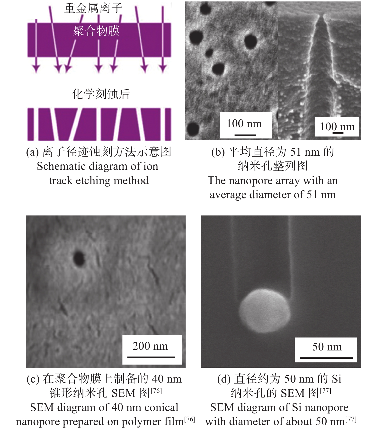
4. 离子径迹刻蚀法
化学刻蚀是微纳加工制造最常见且通用的方法之一,可以实现低成本高效率以及大批量制备。它不需要昂贵的设备且可以一次性并行制备大量的纳米孔(纳米孔阵列)。离子径迹刻蚀法的原理是通过将高能重金属离子射入聚合物膜来产生径迹,然后用刻蚀剂刻蚀被重离子辐照的薄膜,轨道区域的刻蚀速率大于非轨道区域的刻蚀速率,从而形成孔隙[30]。通过离子径迹刻蚀法,已经成功在许多相对便宜的材料中制备了纳米孔,如聚酰亚胺[72]、聚碳酸酯[73]和氮化硅[28]。此外,由于聚合物膜的厚度通常为几微米,因此孔隙形态通常为具有高纵横比的圆锥形。然而,用于通过聚焦离子束和高能电子束刻蚀方法制造纳米孔的Si3N4、SiO2和石墨烯膜的厚度范围从亚纳米到数百纳米。具有高纵横比的不对称结构已被用于模拟蛋白质或生物通道,并研究离子电流整流特性[74]。利用离子径迹刻蚀法制备的固态纳米孔如图6所示。
ZHANG等[28]用高能Br + (81 MeV)刻蚀氮化硅纳米孔,纳米孔直径可以通过改变二氧化硅重离子径迹的氢氟酸刻蚀时间来控制。APEL等[75]制造了平均尺寸为51 nm、孔密度为3 × 109 cm−2的锥形纳米孔阵列,如图6b所示。SIWY等[30]使用离子径迹刻蚀方法获得了最小直径为2 nm的锥形纳米孔。
纳米孔的形状主要依赖于制备过程中辐照及刻蚀的条件参数,适用于制备通道较长(约在微米级别)的高密度柔性纳米孔阵列。然而,离子径迹刻蚀法只能在聚合物膜中制造纳米孔,对于聚合物纳米孔而言,在刻蚀过程中可能会在聚合物薄膜表面引入负电荷,因此会排斥带同种电荷的生物分子(如DNA、BSA等),导致纳米孔捕获生物分子的效率下降。由于离子轨道的不可控,容易出现孔径分布不均匀现象。此外,它需要昂贵的重离子加速度计,制约了固态纳米孔的制造与应用。
常见的高能束加工固态纳米孔的方法如表1所示,包括适用材料、可加工的孔径及方法的优缺点。
表 1 常见的高能束加工固态纳米孔的方法Table 1. Common methods of machining solid-state nanopores with high-energy beams5. 结语
本文主要介绍了高能电子束、聚焦离子束、激光刻蚀、离子径迹刻蚀等4种高能束固态纳米孔制备的工作原理及其制造方法的优缺点。高能电子束和聚焦离子束的优点在于高精度,具有原子分辨率,制造的纳米孔有望应用于DNA测序、蛋白质测序、分子筛选、光调制、离子逻辑器件以及海水淡化,但其制造依赖于昂贵的设备。激光刻蚀是一种以无污染、高效率的方式在薄膜中制备纳米孔的方法,但尺寸精度控制较差。离子径迹刻蚀法具有低成本、高效率的特点,能满足可扩展大批量制造的要求,但其孔径分布不均匀。
每一种制造方法都有其独特的优势,也有不同的应用场景。电子束和离子束制造方法是最具特点和最直接的方法,已经被几个独立的研究小组应用于广泛的材料。但对于批量生产,激光刻蚀和离子径迹刻蚀更有优势,因为这些技术只需要低成本的设备,因此在经济上是可并行的。
随着大规模并行检测和小分子检测的需求,应开发和优化一种快速且经济高效的可扩展技术,用于制造具有小尺寸(<10 nm)和更好均匀性的有序纳米孔阵列。尽管仍有许多挑战,但固态纳米孔将继续是一个活跃和有吸引力的研究领域。随着先进微纳制造技术和新理论研究的开展,固态纳米孔制造将成本更低、效率更高、应用范围更广。
-
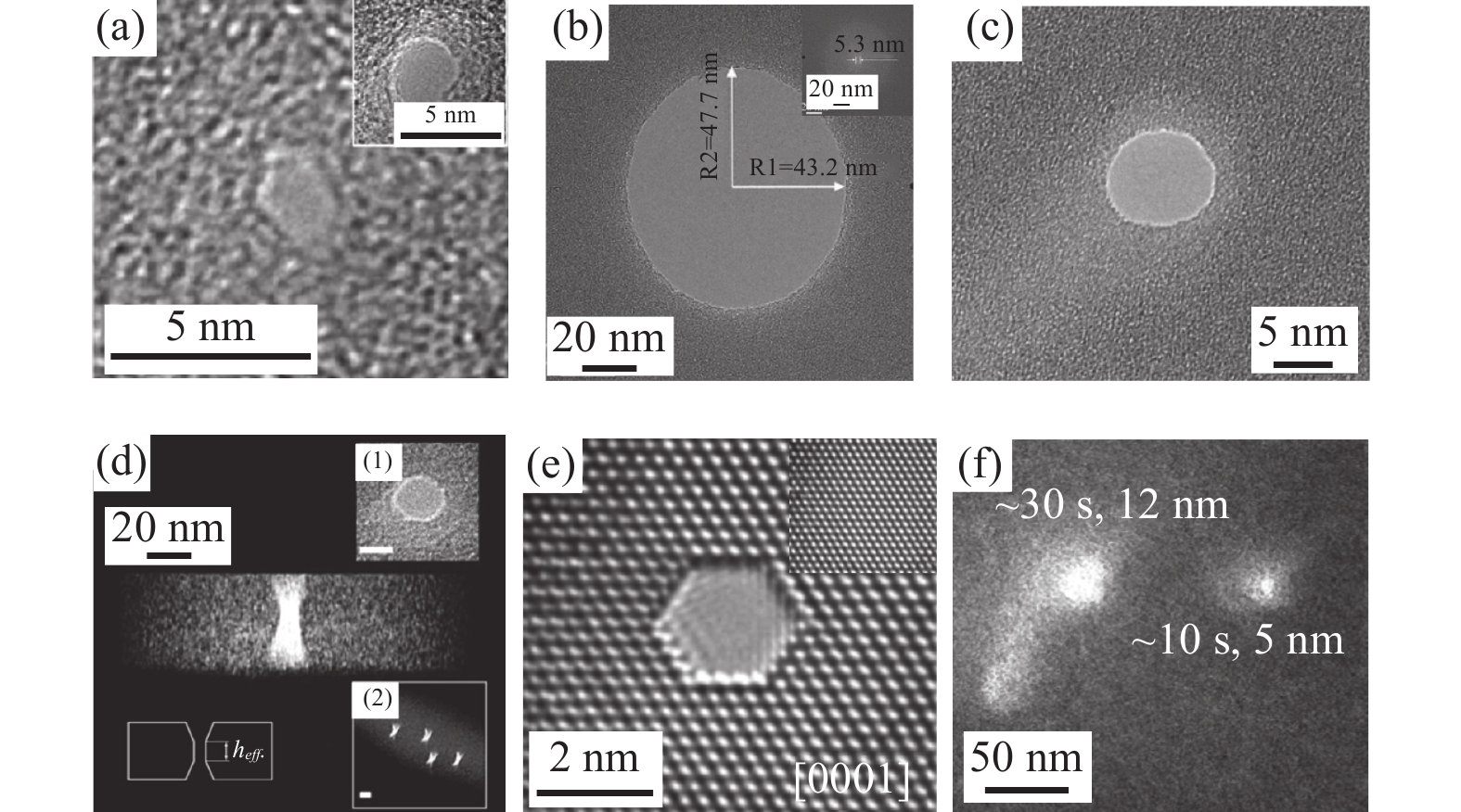
图 3 利用高能电子束制造技术制备的各种固态纳米孔的SEM图和TEM图
(a)利用高能电子束在SiO2薄膜上刻蚀初始直径约为6 nm的纳米孔(右上角插图),后经高强度TEM照射后孔径缩小至2 nm[15];(b)利用FIB制备初始直径约90 nm Si3N4孔,后经SEM辐照将孔缩小至5.3 nm[41](右上角插图);(c)利用聚焦电子束刻蚀得到纳米孔[51];(d)50 nm厚Si3N4膜上直径约7 nm纳米孔的横截面示意图,7 nm孔的俯视图(1),2 nm × 2 nm孔阵列倾斜视图(2)[52];(e)孔径为3.3 nm的Mg纳米孔[47],后在散焦电子束辐照下完全闭合(右上插图);(f)利用SEM制备出孔径小于5 nm的绝缘纳米孔[49]。
Figure 3. SEM and TEM diagrams of various solid nanopores prepared by high-energy electron beam manufacturing technology
(a) A nanopore with an initial diameter of about 6 nm is etched on the SiO2 film by high-energy electron beam (the illustration in the upper right corner), and then the pore size is reduced to 2 nm after high intensity TEM irradiation[15]; (b) The holes with initial diameter of about 45 nm Si3N4 were prepared by FIB, and then the hole was reduced to 5.3 nm [41] by SEM irradiation (illustration in the upper right corner); (c) Nanoholes are obtained by focused electron beam etching[51]; (d) Cross-sectional diagram of about 7 nm diameter nanopore on 50 nm thick Si3N4 film, top view of 7 nm hole (1), 2 nm× 2 nm inclined view of nanopore array (2)[52]; (e) Mg nanopore with a diameter of 3.3 nm [47] was completely closed under the irradiation of defocused electron beam (upper right illustration); (f) Insulated nanopores with aperture less than 5 nm were prepared by SEM[49].
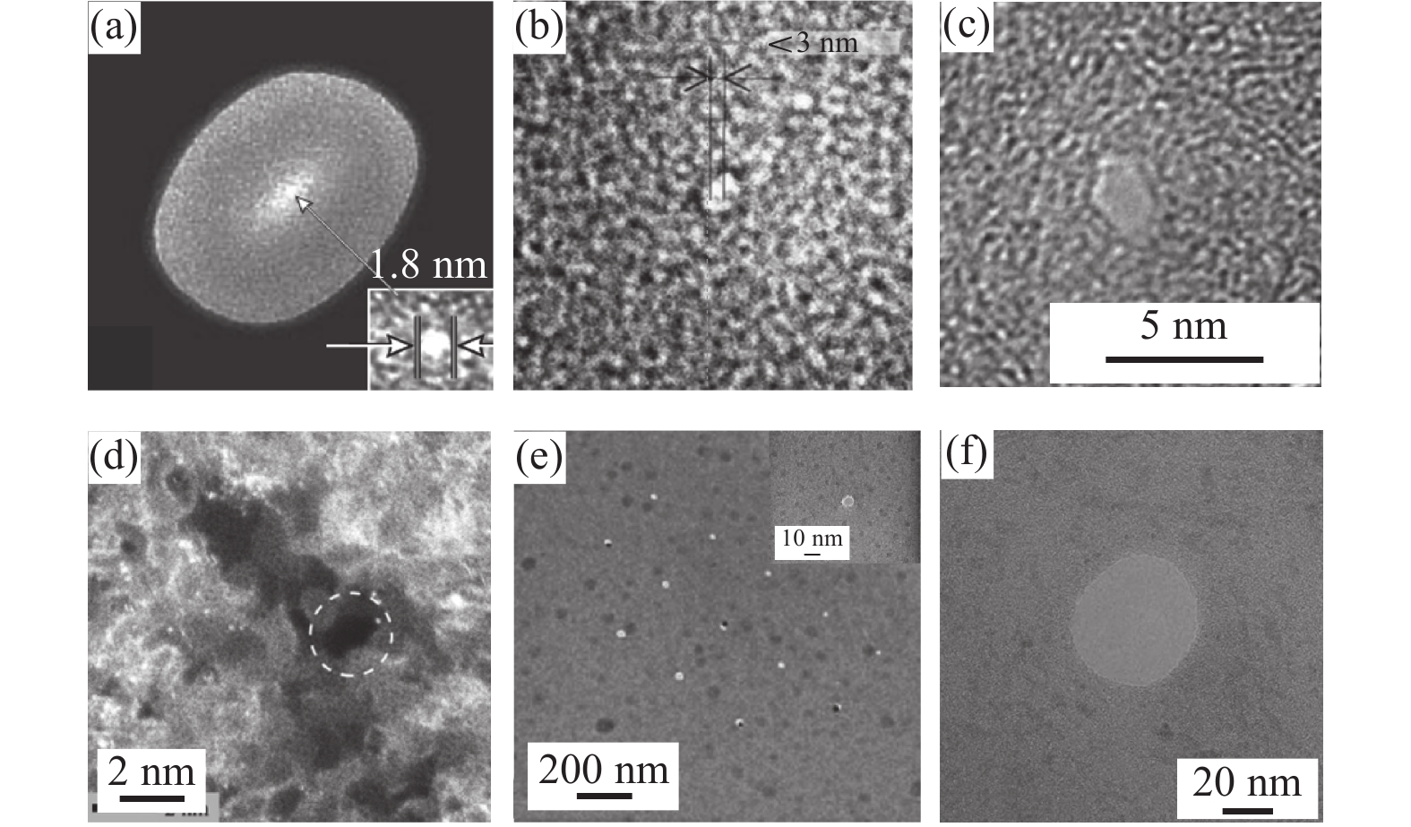
图 4 聚焦离子束制造技术制备的固态纳米孔的SEM和TEM图
(a) Ar + 离子制备Si3N4纳米孔[13]; (b) Ga + 离子制备SiC纳米孔[57];(c)聚焦离子束制备的4 nm Si3N4纳米孔[55];(d) He + 离子制备CNM纳米孔[30];(e)He + 离子制备Si3N4阵列孔和单孔(右上角插图)[65];(f)石墨烯纳米孔[63]。
Figure 4. SEM and TEM images of solid nanopores prepared by focused ion beam manufacturing technology
(a) Preparation of Si3N4 nanopore by Ar + ion[13]; (b) Preparation of SiC nanopore by Ga + ion[57]; (c) 4 nm Si3N4 nanopore prepared by focused ion beam[55]; (d) CNM nanopore prepared by He + ion[30]; (e) Si3N4 array holes and single holes prepared by He + ions (illustration in the upper right corner)[65]; (f) Graphene nanopore[63].
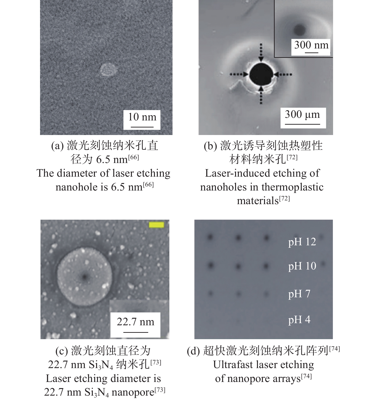
图 5 激光刻蚀技术制备的固态纳米孔的SEM和TEM图
Figure 5. SEM and TEM images of solid-state nanoholes prepared by laser etching technology
表 1 常见的高能束加工固态纳米孔的方法
Table 1. Common methods of machining solid-state nanopores with high-energy beams
 下载: 导出CSV
-
[1] KASIANOWICZ J J, BRANDIN E, BRANTON D, et al. Characterization of individual polynucleotide molecules using a membrane channel [J]. Proceedings of the National Academy of Sciences, 1996,1996,93(24):13770-13773. doi: 10.1073/PNAS.93.24.13770 [2] COULTER W H. Means for counting particles suspended in a fluid: US2656508A [P]. 1953-10-20. [3] KASIANOWICZ J J, ROBERTSON J W, CHAN E R, et al. Nanoscopic porous sensors [J]. Annual Review of Analytical Chemistry,2008,1:737-766. doi: 10.1146/ANNUREV.ANCHEM.1.031207.112818 [4] LI J, STEIN D, MCMULLAN C, et al. Ion-beam sculpting at nanometre length scales [J]. Nature,2001,412(6843):166-169. doi: 10.1038/35084037 [5] JIANG X, ZANG M, LI F, et al. Highly sensitive detection of paraquat with pillar[5]arene as an aptamer in α-hemolysin nanopore [J]. Materials Chemistry Frontiers,2021,5(18):7032-7040. doi: 10.1039/D1QM00875G [6] PAVLENOK M, NIEDERWEIS M. Hetero-oligomeric MspA pores in Mycobacterium smegmatis [J]. Fems Microbiology Letters,2016,363(7):fnw046. doi: 10.1093/femsle/fnw046 [7] HUANG G, VOET A, MAGLIA G. FraC nanopores with adjustable diameter identify the mass of opposite-charge peptides with 44 dalton resolution [J]. Nature Communications,2019,10(1):1-10. doi: 10.1038/s41467-019-08761-6 [8] 段静. MspA蛋白质纳米传感器的制备及其单分子检测应用 [D]. 西安: 西北大学, 2016.DUAN Jing. Preparation and application of the MspA protein nanosensor in single molecule detection [D]. Xi'an: Northwest University, 2016. [9] AKESON M, BRANTON D, KASIANOWICZ J J, et al. Microsecond time-scale discrimination among polycytidylic acid, polyadenylic acid, and polyuridylic acid as homopolymers or as segments within single RNA molecules [J]. Biophysical Journal,1999,77(6):3227-3233. doi: 10.1016/S0006-3495(99)77153-5 [10] ZHANG L, BURNS N, JORDAN M, et al. Macromolecule sensing and tumor biomarker detection by harnessing terminal size and hydrophobicity of viral DNA packaging motor channels into membranes and flow cells [J]. Biomaterials Science,2021,10(1):167-177. doi: 10.1039/D1BM01264A [11] JAIN M, FIDDES I T, MIGA K H, et al. Improved data analysis for the MinION nanopore sequencer [J]. Nature Methods,2015,12(4):351-356. doi: 10.1038/nmeth.3290 [12] VENTA K, SHEMER G, PUSTER M, et al. Differentiation of short, single-stranded DNA homopolymers in solid-state nanopores [J]. ACS Nano,2013,7(5):4629-4636. doi: 10.1021/nn4014388 [13] STORM A J, CHEN J H, LING X S, et al. Fabrication of solid-state nanopores with single-nanometre precision [J]. Nature Materials,2003,2(8):537-540. doi: 10.1038/nmat941 [14] STORM A J, CHEN J H, LING X S, et al. Electron-beam-induced deformations of SiO2 nanostructures [J]. Journal of Applied Physics,2005,98(1):14307. doi: 10.1063/1.1947391 [15] VENKATESAN B M, DORVEL B, YEMENICIOGLU S, et al. Highly sensitive, mechanically stable nanopore sensors for DNA analysis [J]. Advanced Materials,2009,21(27):2771-2776. doi: 10.1002/adma.200803786 [16] GARAJ S, HUBBARD W, REINA A, et al. Graphene as a subnanometre trans-electrode membrane [J]. Nature,2010,467(7312):190-193. doi: 10.1038/NATURE09379 [17] LARKIN J, HENLEY R, BELL D C, et al. Slow DNA transport through nanopores in hafnium oxide membranes [J]. ACS Nano,2013,7(11):10121-10128. doi: 10.1021/nn404326f [18] SHIM J, RIVERA J A, BASHIR R. Electron beam induced local crystallization of HfO2 nanopores for biosensing applications [J]. Nanoscale,2013,5(22):10887-10893. doi: 10.1039/C3NR02608F [19] LIU K, FENG J, KIS A, et al. Atomically thin molybdenum disulfide nanopores with high sensitivity for DNA translocation [J]. ACS Nano,2014,8(3):2504-2511. doi: 10.1021/nn406102h [20] DANDA G, MASIH D P, CHOU Y C, et al. Monolayer WS2 nanopores for DNA translocation with light-adjustable sizes [J]. ACS Nano,2017,11(2):1937-1945. doi: 10.1021/acsnano.6b08028 [21] APEL P. Track etching technique in membrane technology [J]. Radiation Measurements,2001,34(1):559-566. doi: 10.1016/S1350-4487(01)00228-1 [22] DENG Y, HUANG Q, ZHAO Y, et al. Precise fabrication of a 5 nm graphene nanopore with a helium ion microscope for biomolecule detection [J]. Nanotechnology,2017,28(4):045302. doi: 10.1088/1361-6528/28/4/045302 [23] XIA D, HUYNH C, MCVEY S, et al. Rapid fabrication of solid-state nanopores with high reproducibility over a large area using a helium ion microscope [J]. Nanoscale,2018,10(11):5198-5204. doi: 10.1039/C7NR08406D [24] LI W, BELL N A, HERNANDEZ-AINSA S, et al. Single protein molecule detection by glass nanopores [J]. ACS Nano,2013,7(5):4129-4134. doi: 10.1021/nn4004567 [25] SHIM J, KIM Y, HUMPHREYS G I, et al. Nanopore-based assay for detection of methylation in double-stranded DNA fragments [J]. ACS Nano,2015,9(1):290-300. doi: 10.1021/nn5045596 [26] QIU Y. Optimal voltage for nanoparticle detection with thin nanopores [J]. Analyst,2018,143(19):4638-4645. doi: 10.1039/c8an01270a [27] GUO W, CAO L, XIA J, et al. Energy harvesting with single-ion-selective nanopores: A concentration-gradient-driven nanofluidic power source [J]. Advanced Functional Materials,2010,20(8):1339-1344. doi: 10.1002/adfm.200902312 [28] ZHANG W M, WANG Y G, LI J, et al. Controllable shrinking and shaping of silicon nitride nanopores under electron irradiation [J]. Applied Physics Letters,2007,90(16):163102. doi: 10.1063/1.2723680 [29] EMMRICH D, BEYER A, NADZEYKA A, et al. Nanopore fabrication and characterization by helium ion microscopy [J]. Applied Physics Letters,2016,108(16):285310. doi: 10.1063/1.4947277 [30] SIWY Z, FULINSKI A. Fabrication of a synthetic nanopore ion pump [J]. Physical Review Letters,2002,89(19):198103. doi: 10.1103/PhysRevLett.89.198103 [31] KWOK H, BRIGGS K, TABARD-COSSA V. Nanopore fabrication by controlled dielectric breakdown [J]. PLoS One,2014,9(3):e92880. doi: 10.1371/journal.pone.0092880 [32] BELLO J, SHIM J. Solid-state nanopore fabrication in LiCl by controlled dielectric breakdown [J]. Biomed Microdevices,2018,20(2):38. doi: 10.1007/s10544-018-0281-9 [33] YUAN Z, WANG C, YI X, et al. Solid-state nanopore [J]. Nanoscale Research Letters,2018,13(1):56. doi: 10.1186/s11671-018-2463-z [34] LIANG J, CHIK H, YIN A, et al. Two-dimensional lateral superlattices of nanostructures: Nonlithographic formation by anodic membrane template [J]. Journal of Applied Physics,2002,91(4):2544-2546. doi: 10.1063/1.1433173 [35] AYUB M, IVANOV A, HONG J, et al. Precise electrochemical fabrication of sub-20 nm solid-state nanopores for single-molecule biosensing [J]. Journal of Physics: Condensed Matter,2010,22(45):454128. doi: 10.1088/0953-8984/22/45/454128 [36] WU M Y, KRAPF D, ZANDBERGEN M, et al. Formation of nanopores in a SiN/SiO2 membrane with an electron beam [J]. Applied Physics Letters,2005,87(11):113106. doi: 10.1063/1.2043247 [37] SHIN J W, LEE J Y, OH D H, et al. Shrinkage and expansion mechanisms of SiO2 elliptical membrane nanopores [J]. Applied Physics Letters,2008,93(22):221903. doi: 10.1063/1.3027062 [38] KIM M J, WANUNU M, BELL D C, et al. Rapid fabrication of uniformly sized nanopores and nanopore arrays for parallel DNA analysis [J]. Advanced Materials,2006,18(23):3149-3153. doi: 10.1002/ADMA.200601191 [39] CHANG H, IQBAL S M. Fabrication and characterization of solid-state nanopores using a field emission scanning electron microscope [J]. Applied Physics Letters,2006,88(10):103109. doi: 10.1063/1.2179131 [40] YUAN Z, LEI X, WANG C. Controllable fabrication of solid state nanopores array by electron beam shrinking [J]. International Journal of Machine Tools and Manufacture,2020,159(SI):103623. doi: 10.1016/J.IJMACHTOOLS.2020.103623 [41] GOLDSTEIN J I, NEWBURY, D E, ECHLIN P, et al. Scanning electron microscopy and X-ray microanalysis: A text for biologists, materials scientists, and geologists [M]. New York: Springer, 1981. [42] HE K, ROBERTSON A W, GONG C, et al. Controlled formation of closed-edge nanopores in graphene [J]. Nanoscale,2015,7(27):11602-11610. doi: 10.1039/c5nr02277k [43] XU T, XIE X, SUN L. Fabrication of nanopores using electron beam [C]//IEEE Computer Society. The 8th Annual IEEE International Conference on Nano/Micro Engineered and Molecular Systems. Suzhou: IEEE Computer Society, 2013. [44] KIM H M, LEE M H, KIM K B. Theoretical and experimental study of nanopore drilling by a focused electron beam in transmission electron microscopy [J]. Nanotechnology,2011,22(27):275303. doi: 10.1088/0957-4484/22/27/275303 [45] PATTERSON N, ADAMS D P, HODGES V C, et al. Controlled fabrication of nanopores using a direct focused ion beam approach with back face particle detection [J]. Nanotechnology,2008,19(23):235304. doi: 10.1088/0957-4484/19/23/235304 [46] WU S, CAO F, ZHENG H, et al. Fabrication of faceted nanopores in magnesium [J]. Applied Physics Letters,2013,103(24):243101. doi: 10.1063/1.484515 [47] RIGO E, DONG Z, PARK J H, et al. Measurements of the size and correlations between ions using an electrolytic point contact [J]. Nature Communications,2019,10(1):1-13. doi: 10.1038/s41467-019-10265-2 [48] SPINNEY P S, HOWITT D G, SMITH R L, et al. Nanopore formation by low-energy focused electron beam machining [J]. Nanotechnology,2010,21(37):375301. doi: 10.1088/0957-4484/21/37/375301 [49] FISCHBEIN M D, DRNDIĆ M. Sub-10 nm device fabrication in a transmission electron microscope [J]. Nano Letters,2007,7(5):1329-1337. doi: 10.1021/nl0703626 [50] TRAVERSI F, RAILLON C, BENAMEUR S M, et al. Detecting the translocation of DNA through a nanopore using graphene nanoribbons [J]. Nat Nanotechnol,2013,8(12):939-945. doi: 10.1038/nnano.2013.240 [51] STEIN D, LI J, GOLOVCHENKO J A. Ion-beam sculpting time scales [J]. Physical Review Letters,2002,89(27):276106. doi: 10.1103/PhysRevLett.89.276106 [52] HENG J B, HO C, KIM T, et al. Sizing DNA using a nanometer-diameter pore [J]. Biophysical Journal,2004,87(4):2905-2911. doi: 10.1529/biophysj.104.041814 [53] YANG J, FERRANTI D C, STERN L A, et al. Rapid and precise scanning helium ion microscope milling of solid-state nanopores for biomolecule detection [J]. Nanotechnology,2011,22(28):285310. doi: 10.1088/0957-4484/22/28/285310 [54] KUAN A T, GOLOVCHENKO J A. Nanometer-thin solid-state nanopores by cold ion beam sculpting [J]. Applied Physics Letters,2012,100(21):213104. doi: 10.1063/1.4719679 [55] GIERAK J, MADOURI A, BIANCE A, et al. Sub-5 nm FIB direct patterning of nanodevices [J]. Microelectronic Engineering,2007,84(5/6/7/8):779-783. doi: 10.1016/j.mee.2007.01.059 [56] 袁志山. 基于固体纳米孔的 DNA 分子检测器件设计与制造 [D]. 南京: 东南大学, 2016.YUAN Zhishan. Design and fabrication of DNA molecule detection devices based on solid-state nanopores [D]. Nanjing: Southeast University, 2016. [57] 武灵芝, 吴宏文, 刘丽萍, 等. 基于聚焦离子束的氮化硅纳米孔的制备和表征 [J]. 生物物理学报,2013(3):203-212.WU Lingzhi, WU Hongwen, LIU Liping, et al. Fabrication and characterization of solid nanopores with silicon nitride membranes by focus ion beam [J]. Acta Biophysica Sinica,2013(3):203-212. [58] HEMAMOUCHE A, MORIN A, BOURHIS E, et al. FIB patterning of dielectric, metallized and graphene membranes: A comparative study [J]. Microelectronic Engineering,2014,121:87-91. doi: 10.1016/j.mee.2014.03.020 [59] MARSHALL M M, YANG J, HALL A R. Direct and transmission milling of suspended silicon nitride membranes with a focused helium ion beam [J]. Scanning,2012,34(2):101-106. doi: 10.1002/sca.21003 [60] SAWAFTA F, CARLSEN A, HALL A R. Membrane thickness dependence of nanopore formation with a focused helium ion beam [J]. Sensors (Switzerland),2014,14(5):8150-8161. doi: 10.3390/s140508150 [61] 袁志山, 戴敏, 郑李娟, 等. 石墨烯纳米孔传感器制造与单分子过孔形态检测 [J]. 机械工程学报,2022,58(5):190-197. doi: 10.3901/JME.2022.05.190YUAN Zhishan, DAI Min, ZHENG Lijuan, et al. Graphene nanopore sensor fabrication and single molecule translocation form detection [J]. Journal of Mechanical Engineering,2022,58(5):190-197. doi: 10.3901/JME.2022.05.190 [62] HAYASHI T, ARIMA K, YAMASHITA N, et al. Nanopore fabrication of two-dimensional materials on SiO2 membranes using he ion microscopy [J]. IEEE Transactions on Nanotechnology,2018,17(4):727-730. doi: 10.1109/TNANO.2018.2840721 [63] GILBOA T, ZREHEN A, GIRSAULT A, et al. Optically-monitored nanopore fabrication using a focused laser beam [J]. Scientific Reports,2018,8(1):9765. doi: 10.1038/s41598-018-28136-z [64] ZHANG J S K, MIDORIKAWA K. Laser-induced plasmaassisted ablation of fused quartz using the fourth harmonic of a Nd+: YAG laser [J]. Applied Physics A,1998,67:545-549. doi: 10.5772/61567 [65] QIN L, HUANG Y, XIA F, et al. 5 nm nanogap electrodes and arrays by super-resolution laser lithography [J]. Nano Letters,2020,20(7):4916-4923. doi: 10.1021/acs.nanolett.0c00978 [66] GAN Z, CAO Y, EVANS R A, et al. Three-dimensional deep sub-diffraction optical beam lithography with 9 nm feature size [J]. Nature Communication,2013,4:2061. doi: 10.1038/ncomms3061 [67] LIN Z, LIU H, JI L, et al. Realization of approximately 10 nm features on semiconductor surfaces via femtosecond laser direct patterning in far field and in ambient air [J]. Nano Letters,2020,20(7):4947-4952. doi: 10.1021/acs.nanolett.0c01013 [68] LI Z Z, WANG L, FAN H, et al. O-FIB: Far-field-induced near-field breakdown for direct nanowriting in an atmospheric environment [J]. Light Sci Appl,2020,9(1):41. doi: 10.1038/s41377-020-0275-2 [69] WU S, Park S R, LING X S. Lithography-free formation of nanopores in plastic membranes using laser heating [J]. Nano Letters,2006,6(11):2571-2576. doi: 10.1021/nl0619498 [70] LU Y, KAI L, YANG Q, et al. Laser fabrication of nanoholes on silica through surface window assisted nano-drilling (SWAN) [J]. Nanomaterials,2021,11(12):3340. doi: 10.3390/nano11123340 [71] GILBOA T, ZVULONI E, ZREHEN A, et al. Automated, ultra‐fast laser‐drilling of nanometer scale pores and nanopore arrays in aqueous solutions [J]. Advanced Functional Materials,2019,30(18):1900642. doi: 10.1002/adfm.201900642 [72] SIWY Z, DOBREV D, NEUMANN R, et al. Electro-responsive asymmetric nanopores in polyimide with stable ion-current signal [J]. Applied Physics A: Materials Science & Processing,2003,76(5):781-785. doi: 10.1007/s00339-002-1982-7 [73] APEL P Y, KORCHEV Y E, SIWY Z, et al. Diode-like single-ion track membrane prepared by electro-stopping [J]. Nuclear Instruments and Methods in Physics Research (Section B),2001,184(3):337-346. doi: 10.1016/S0168-583X(01)00722-4 [74] SIWY Z S. Ion-current rectification in nanopores and nanotubes with broken symmetry [J]. Advanced Functional Materials,2006,16(6):735-746. doi: 10.1002/adfm.200500471 [75] APEL P Y, BLONSKAYA I V, DMITRIEV S N, et al. Fabrication of nanopores in polymer foils with surfactant-controlled longitudinal profiles [J]. Nanotechnology,2007,18(30):305302. doi: 10.1088/0957-4484/18/30/305302 [76] HARRELL C C, CHOI, Y, HOME L P, et al. Resistive-pulse DNA detection with a conical nanopore sensor [J]. Langmuir,2006,22(25):10837-10843. doi: 10.1021/la061234k [77] TSUJINO K, MATSUMURA M. Morphology of nanoholes formed in silicon by wet etching in solutions containing HF and H2O2 at different concentrations using silver nanoparticles as catalysts [J]. Electrochimica Acta,2007,53(1):28-34. doi: 10.1016/j.electacta.2007.01.035 -

 下载:
下载:


 点击查看大图

计量
- 文章访问数: 1421
- HTML全文浏览量: 505
- PDF下载量: 176
- 被引次数: 0
 邮件订阅
邮件订阅 RSS
RSS